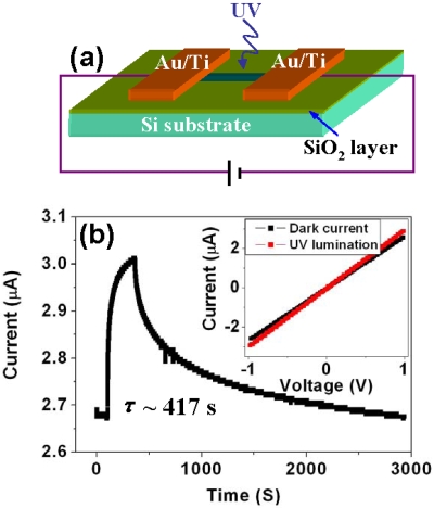
Figure 1.
(a) Schematic of a ZnO NW UV NS device structure with Ohmic contacts. (b) Photon response of a ZnO NW UV NS, made using Ti/Au electrodes and at a bias of 1 V, when illuminated by ∼30 μW∕cm2 365 nm UV source. The inset shows the corresponding I-V characteristics in dark or under UV illumination.

