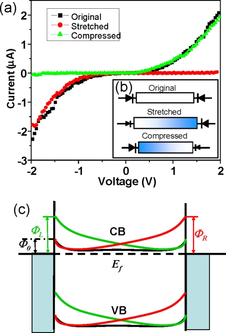
Figure 3.
Strain induced change of I-V characteristic from symmetric to asymmetric (diode). (a) Changes of transport characteristics of a Ag/ZnO-nanowire/Ag device from symmetric I-V characteristic (black) to asymmetric rectifying behavior when stretching (red) and compressing (green) the wire. (b) Circuit diagram models of the device in corresponding to the observed I-V curves, different sizes of diode symbol are used to illustrate the asymmetric Schottky contacts at the two ends of the nanowire. The blue side is the negative potential side, and the other side is the positive side. (c) Schematic energy band diagrams illustrating the changes of Schottky barriers from symmetric (black) to asymmetric under tensile strain (red) and compressive strain (green), in corresponding to the I-V curves in (a).

