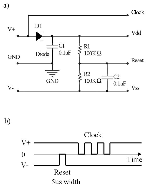
Fig 2.
Decoder and control signal of the dual-supply design. a) Decoder circuit b) Control signal and its timing for configuring the counter: First, the reset pulse is generated by temporarily turning off V−. Then, the clock signal, embedded in V+, is applied. Once an active channel of the multiplexer is configured, the stimulating current can be passed from the shared contact through the active channel in the electrode to GND.

