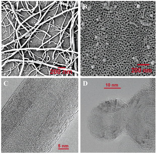
Figure 1.
Scanning electron microscopy (SEM) images and high-resolution transmission electron microscopy (HRTEM) images of carbon nanomaterials used in this study. (A) SEM image of multiwalled carbon nanotubes (scale bar = 200 nm). (B) SEM image of carbon nano-onions (scale bar = 200 nm). (C) HRTEM images of multiwalled carbon nanotubes (MWCNTs) (scale bar = 5 nm). (D) HRTEM images of multiwalled carbon nano-onions (MWCNO) (scale bar = 10 nm).

