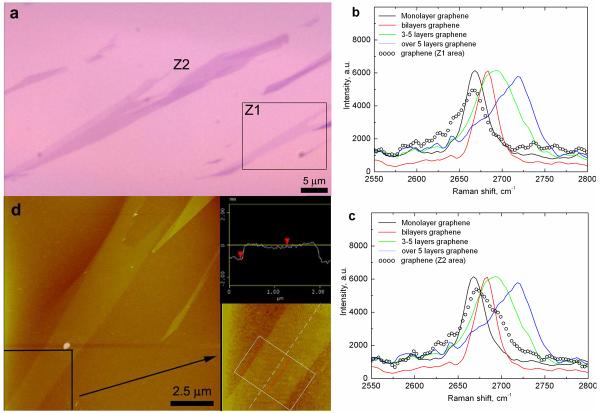
Figure 1.
a) Optical image of the covalently immobilized graphene films on silicon wafer; b), c) Raman spectra of the covalently immobilized graphene film in Z1 (b), and Z2 (c) region (open circle curves), and physisorbed graphene on wafer prepared by the Scotch tape method (solid curves), λlaser = 532 nm; d) AFM image of the Z1 region. Inset is the magnified image of the area indicated by the box and arrow in d), and the sectional analysis showing the thickness of the film to be 0.84 nm.

