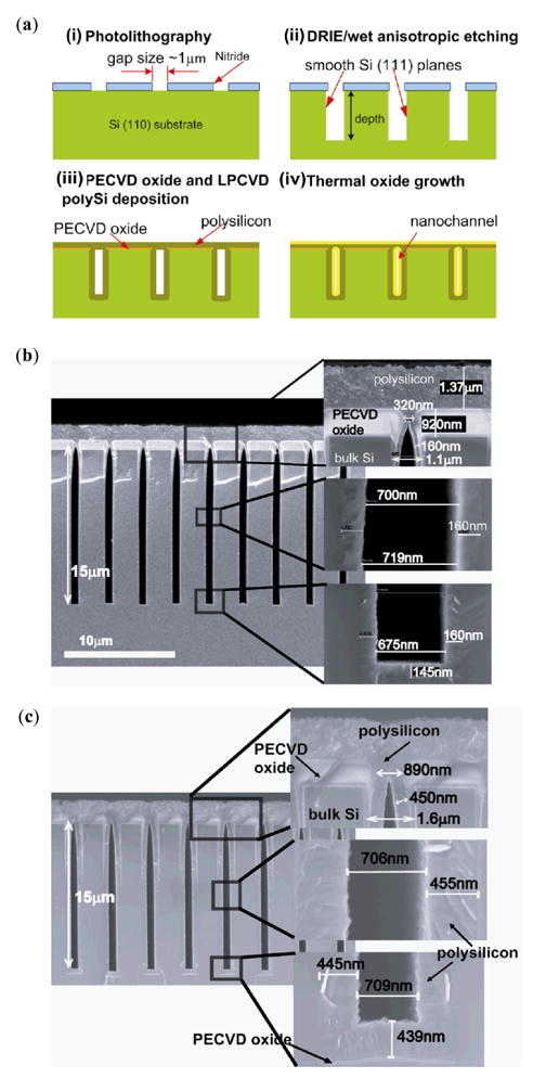
Figure 4.

Modified approach for fabricating embedded vertical nanochannels. (a) Schematic diagram of fabrication process. (i) patterning channels by standard photolithography; (ii) etching by either DRIE or anisotropic wet etching (KOH); (iii) depositing PECVD oxide and conformal LPCVD polysilicon to seal trenches sequentially; (iv) growing thermal oxide to decreases the gap size. (b,c) Cross-sectional SEM images of 15 μm deep trenches deposited with 900 nm thick PECVD oxide and 1.37 μm thick LPCVD polysilicon sequentially. The gap size uniformly changes from 1.6 μm to 706 nm (b) and from 1.1 μm to 700 nm (c) after deposition. It shows that their final gap after LPCVD polysilicon deposition becomes almost the same although their initial gap size differs by 0.5 μm.
