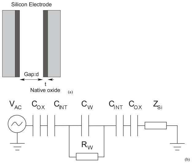
Figure 4.
(a) The electrodes are modeled as capacitors with gap d filled with media and the dielectric native oxide of thickness t. (b) Lumped parameter circuit of the system indicating the electrical double layer capacitance of the interface CINT, native oxide capacitance COX and components of media impedance CW and RW. ZSi is not part of the electrode but arises due to parasitic impedance in the substrate.

