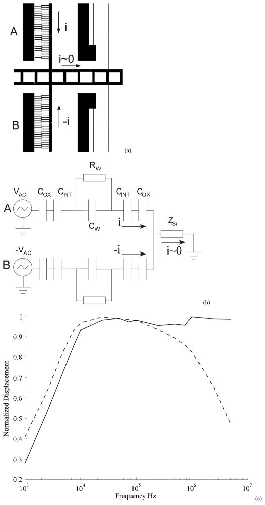
Figure 8.
(a) Electrode geometry layout to achieve the proposed design to minimize substrate current flow by injecting opposing current flows from each electrode (b) Schematic of circuit model indicating the zero current flow through the device and substrate. (c) A comparison of normalized displacement frequency response of a device operated in DI water with signals that are in-phase (dashed) and out-of-phase (continuous) indicates that the displacement in the latter case show reduced attenuation.

