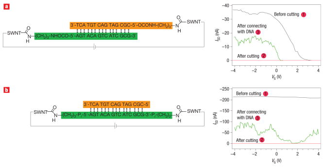
Figure 2. Device characteristics for individual SWNTs connected with DNA.
a,b, Source–drain current versus VG at a constant source –drain voltage (50 mV) before cutting (black curve: 1), after cutting (red curve: 2) and after connection with the DNA sequence shown (green curve: 3), for a semiconducting SWNT device (a) and a metallic SWNT device (b). Guanine, G; cytosine, C; adenine, A; thymine, T.

