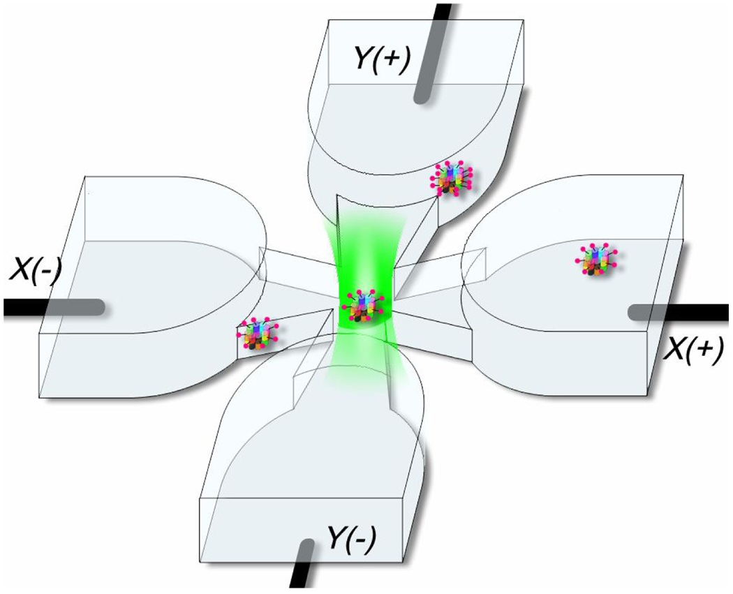
Figure 2.
Cartoon of the microfluidic geometry, showing a labeled protein trapped in the center of the trapping region (not to scale). The microfluidic cell is made of fused silica as previously described [3]. Channels are etched in fused silica wafers, thin in the trapping region, and deep in the regions extending out to the electrodes. The patterned wafer is bonded to a quartz coverslip with a thin layer of sodium silicate solution. The depth of the cell used in this study along the axial direction is 750nm in the trapping region, while the transverse dimensions of the thin trapping region are ~20µmx20µm.

