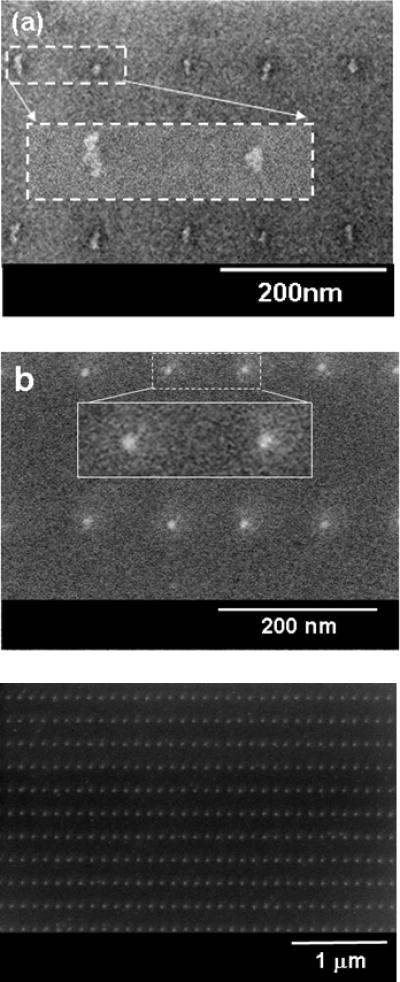
Figure 5.

(a) AuPd dots before annealing. The dots correspond to an initial size of the mold pillars of ~18nm, and angle-evaporated Ti mask of 10 nm thickness. (b) The same dots after annealing. (c) Large area view of an array of annealed dots. An apparent “halo” around the nanodots is often seen on such images. This is probably due to charging of the substrate by the oxygen plasma, which is used to remove the residual PMMA film from these areas.
