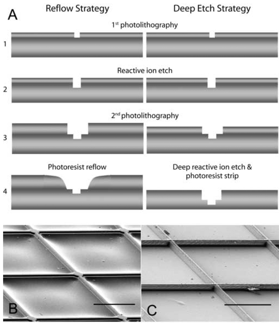
Figure 1. Cartoon illustrating fabrication steps used to produce masters for microcontact printing and scanning electron micrographs of molded PDMS stamps.
(A) Two different strategies – reflow and deep-etch – were used to produce support for the 200-µm long lines connecting to the electrode sites. The pink layers represent photoresist. The gray layers represent the silicon wafers. Masters fabricated using resist reflow (B) produced structures containing a sloping base to support the raised surfaces that will be used to transfer proteins to the surfaces of the MEAs. Masters fabricated using the double deep-etch (C) strategy produced raised features on a stepped base. Scale bar = 100 µm.

