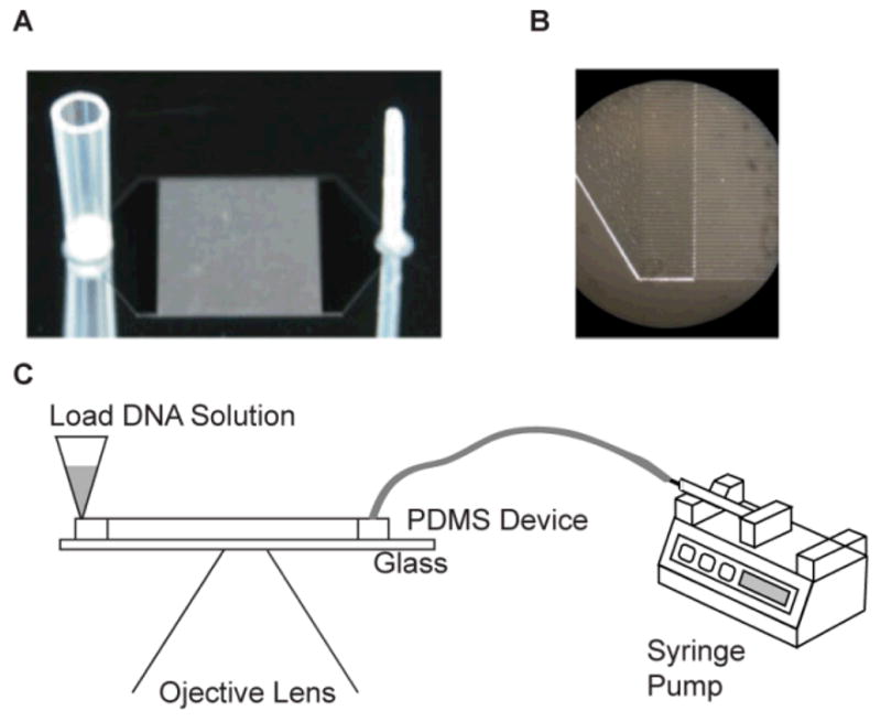
Fig. 2. Experimental Set-Up.

(A) Photograph of a photoresist patterned silicon wafer used to mold silastic replica devices (not shown). Ports were directly molded into silastic devices by gluing a section of a wide bore pipette tip (left) and a Teflon tube (right) to the wafer; attached ports appear mirrored on the wafer. The ports connect via plenums to a rectangular (8 mm × 1 cm) array of 125, 8 mm long square channels [40μm × 40 μm; 40 μm separation]. (B) Close-up micrograph of image (A) detailing plenum/microchannels. (C) Schematic of experimental set-up on an optical microscope. A syringe pump connected to the smaller port (right) of the device controls fluid flow; DNA is loaded through the larger port (left).
