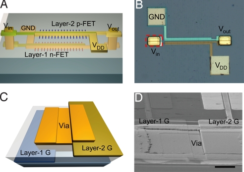
Fig. 1.
The 3D CMOS circuit and vertical interconnection. (A) Schematic of a two-layer CMOS inverter circuit. Layer-1 and layer-2 are constructed with complementary n-type InAs NWs and p-type Ge/Si core/shell NWs, and vertical interconnections are achieved at the two gate electrodes (input) and the two drain electrodes (output). GND denotes electrical ground. (B) Optical microscope image of vertically interconnected CMOS inverter. Red dashed box indicates via interconnection at the input of CMOS inverter. (C) Side tilted-view schematic drawing (rotated 90° counterclockwise of red dashed box in B) of via interconnection at the input of CMOS inverter. (D) Tilted-view SEM image (rotated 90° counterclockwise of red dashed box in B) of via interconnection at the input of CMOS inverter. (Scale bar: 5 μm.)

