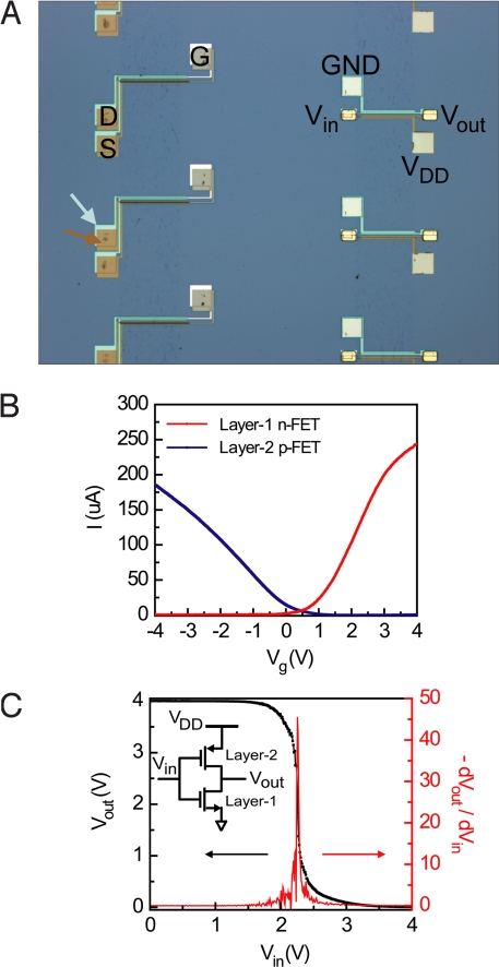
Fig. 2.
Vertically interconnected CMOS inverter. (A) Optical microscope image of isolated n-InAs and p-Ge/Si NW FETs (left column), and two-layer interconnected CMOS inverters (right column). The n-InAs NW FETs were fabricated in layer-1 (light-blue contrast and arrow), and the p-Ge/Si NW FETs were fabricated in layer-2 (light-brown contrast and arrow). (B) I vs. Vg characteristics data recorded from representative InAs layer-1 and Ge/Si layer-2 NW devices with |Vds| = 1 V. The data from the InAs NW FET were recorded before fabrication of the layer-2. (C) Vout vs. Vin (black curve) and gain = dVout/dVin vs. Vin (red curve) for a CMOS inverter at supply voltage, VDD, of 4 V. (Inset) Circuit diagram for the vertically interconnected two-layer CMOS inverter.

