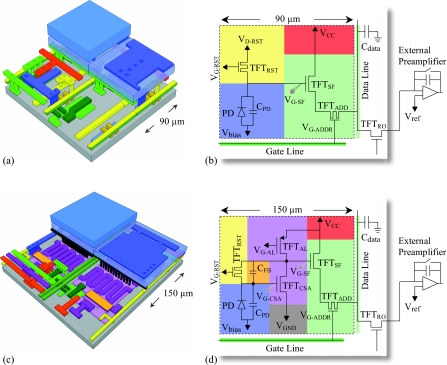
Figure 4.
Illustrations relating the physical structure of the prototype active pixels to their circuit diagrams, with color coding to indicate the correspondence between parts of the circuit and their physical implementation in the pixel. Three-dimensional drawings of the detailed structure of (a) PSI-2 and (c) PSI-3 pixels. Each drawing illustrates four adjoining pixels and reveals varying degree of detail. Note that dimensions in the direction perpendicular to the substrate have been exaggerated for clarity of presentation. Schematic circuit diagrams for prototype arrays (b) PSI-2 and (d) PSI-3. For each diagram, the dashed line delineates an individual pixel from other elements on the array. Each pixel design incorporates: a photodiode structure, PD, with capacitance per pixel of CPD (in blue); a dual-gate addressing transistor TFTADDR and a source-follower transistor, TFTSF, providing an amplification stage (both shown in light green); a reset transistor, TFTRST, and its control lines (in yellow); and a readout transistor, TFTRO, located on the periphery of the array and used to allow integration of the amplified signal on the data line capacitance, Cdata, prior to sampling by an external preamplifier. For PSI-3, additional circuit elements include: a common-source amplifier transistor, TFTCSA, and an active load transistor, TFTAL, which together provide the first of two stages of amplification (in purple); a feedback capacitor, CFB, (in orange), which serves as the pixel storage capacitor; and a ground line (in dark gray). Vbias represents the reverse bias voltage externally applied to the photodiode. VD-RST and VG-RST refer to the voltage applied to the drain electrode and gate electrode of TFTRST in the PSI-2 and PSI-3 designs, respectively. Finally note that, for PSI-3, adjacent pixels share common lines which provide supply voltages (i.e., VCC, VG-AL, and VGND along the data line direction and VG-RST along the gate line direction). Values for these voltages are given in Table 2.

