Abstract
We report the synthesis of vertical silicon nanowire array through a two-step metal-assisted chemical etching of highly doped n-type silicon (100) wafers in a solution of hydrofluoric acid and hydrogen peroxide. The morphology of the as-grown silicon nanowires is tunable from solid nonporous nanowires, nonporous/nanoporous core/shell nanowires, and entirely nanoporous nanowires by controlling the hydrogen peroxide concentration in the etching solution. The porous silicon nanowires retain the single crystalline structure and crystallographic orientation of the starting silicon wafer, and are electrically conductive and optically active with visible photoluminescence. The combination of electronic and optical properties in the porous silicon nanowires may provide a platform for the novel optoelectronic devices for energy harvesting, conversion and biosensing.
Nanoscale silicon has attracted considerable interest due to its potential to impact broad areas ranging from electronics, photonics, renewable energy to biomedical sensing.1–3 Significant efforts have been to devoted to develop new silicon nanostructures, including quantum dots, nanowires or porous silicon. Silicon nanowires, in particular, have been the focus on of intensive research over the past decade due to their unique one-dimensional physical morphology and the associated electrical, mechanical and thermal properties.4,5 To date, silicon nanowires have been broadly explored for nanoscale electronics,6,7 flexible large area electronics,8–11 thermoelectrics,12 photovoltaics,13–15 battery electrode,16 and electronic biosensing.17–19 However, with an indirect band gap, silicon nanowires can hardly be explored as an optically active material for functional optoelectronics. On the other hand, silicon quantum dots and porous silicon is well-known for their ability to exhibit luminescence in the visible range due to strong quantum confinement effect, and has attracted significant attention for silicon based optoelectronics including light-emitting diodes and lasers.20–22 A combination of these two features and the formation of both electrically and optically active porous silicon nanowires may open new opportunities for a new generation of silicon based optoelectronics and photoelectrochemical devices.
In general, porous silicon is produced by anodic etching in hydrofluoric (HF)-containing aqueous or organic solutions21 or by chemical etching in nitric acid/hydrofluoric (HNO3/HF) solution.23 Recently, a simple metal-assisted chemical etching method was developed to produce porous silicon with excellent and repeatable optical properties.24 Lately, this method was also adapted to synthesize vertical silicon nanowire arrays in an etchant solution composed of HF and a selected oxidant (hydrogen peroxide (H2O2) and metal salts, such as AgNO3, KAuCl4, K2PtCl6).25–31 Metal-assisted chemical etching method has been broadly studied for the synthesis of silicon nanowires starting from many types of silicon wafers with different doping levels and orientations, such as lightly and highly doped p-type Si (100) and Si (111) wafers,26,27 lightly doped n-type Si(100) and Si(111) wafers,26 Si(110)32 and Si(113)33 wafers. In general, the metal-assisted chemical etching reactions can be classified into two types: one-step reaction in etchant solution containing HF and metal salts30 and two-step reaction which involves the pre-deposition of metal nanoparticles26,27 or patterned metal thin films31 followed by chemical etching in the presence of HF and H2O2.
Despite significant efforts described above, there is no report on the formation of silicon nanowires from highly doped n-type silicon wafers through the metal-assisted chemical etching to date. In this work, we report the formation of vertical silicon nanowire array from highly doped n-type silicon wafers (resistivity 0.008 – 0.02 Ω·cm) using a two-step silver-assisted chemical etching approach. Importantly, by systematically tuning the etching conditions, solid nonporous, nanoporous silicon nanowires or nonporous/nanoporous core/shell nanowires can be obtained. Electrical transport measurements on individual nanowires show the porous nanowires are conductive with expected n-type behavior but a greatly reduced conductivity. Additionally, photoluminescence studies of the porous silicon nanowires shows that they are optically active with a broad emission around 650 nm. The ability to achieve both electrically and optically active nanoporous silicon nanowires can open new opportunities for silicon based electronics, photonics, and photoelectrical devices. As we are preparing the manuscript of this work, we noted that an online publication reported the formation of optically active mesoporous Si nanowires, which is however obtained from highly doped p-type silicon wafers.34
In our experiment, the commercially available n-type Si (100) wafers with resistivities of 0.008–0.02 Ω·cm, 0.3–0.8 Ω·cm, and 1–5 Ω·cm were used as the starting materials. The pieces of the selected silicon wafers were washed by sonication in acetone and isopropanol and dried by nitrogen blow. For a typical reaction, the silicon pieces were immediately immersed in a solution of 0.02 M silver nitrate (AgNO3) and 5 M HF for a controlled duration to produce silicon nanowires. When the resistivity of the n-Si wafers was higher than 0.1 Ω·cm, the well-aligned vertical Si nanowire arrays were readily obtained (supplementary Figure S1A and S1C). TEM images of the nanowires made from n-type Si (100) 0.3–0.8 Ω·cm and 1–5 Ω·cm wafers show continuous single crystalline structure (supplementary Figure S1B and S1D). These observations are consistent with previous studies.26 However, when highly doped n-type Si (100) wafers (resistivity 0.008–0.02 Ω·cm) were used under the same condition, no vertically aligned nanowires can be obtained. In this case, our studies show that the etching on highly doped n-Si wafer was predominantly in parallel to rather than vertical to the wafer surface (supplementary Figure S1E). This finding may explains the reason why there is no report on the formation of silicon nanowire arrays from highly doped n-type silicon wafers using the metal assisted etch to date. The lack of vertical etch in highly doped n-type silicon wafer may be attributed the following reasons. First, previous studies30 suggest that the formation of vertically aligned nanowires in metal assisted etch is due to the confined etch near the silver nanoparticles, in which the silver nanoparticles on silicon surface catalyze the etching reaction around and below them, and thus creates nanopits that confine the silver nanoparcitcles inside them and therefore confine the etching reaction in the nanopits to ensure the etching is predominantly the along vertical direction. In one-step reaction, the silver nanoparticles are nucleated from the solution. The initial nucleation of silver nanoparticles may preferentially occur near defective sites (e.g. around the dopants) where the energy barrier for redox reaction is lower. The highly doped wafers may have too high density of nucleated silver nanoparticles on surface that are in close proximity of each other, and each nanoparticle may not be effectively confined in its own pits to ensure vertical etching. Indeed, our studies on silver nanoparticle nucleation on the variously doped silicon wafers under the same condition show increasing silver nanoparticle density with increasing doping concentration (supplementary Figure S2). Additionally, even if the vertical etch does happen at the initial stage, the existence of many defects (near the dopants) and the availability of a large amount of Ag+ ions in solution may facilitate the deposition of Ag nanoparticles on the side wall, and create new lateral etching pathways that can overcome the vertical etching, and prevent the formation of vertical nanowire arrays. Based on this argument, the vertical nanowire array may be obtained if we can control the amount of Ag+ in the solution. To this end, we have adopted a two-step reaction to grow vertically aligned nanowires from heavily doped n-silicon wafers through the metal-assistant electroless etching method.
In the two step reaction, the pre-cleaned Si pieces were immersed into a buffered oxide etchant for 2 minutes to remove the native oxide layer, and then immediately transferred into an Ag deposition solution containing 4.8 M HF and 0.005 M AgNO3 for 1 min at room temperature. The color of the Si surface changed from dark to colorful, indicating the formation of silver nanoparticles on the surface of silicon pieces. The Ag-deposited silicon pieces were sufficiently rinsed with deionized water to remove extra silver ions and then immediately soaked into an etchant bath composed of 4.8 M HF and various concentrations of H2O2. The typical etching time varies from 30 to 60 minutes. The Ag metal was removed from the resulted nanowires by immersing the Si pieces into a solution of concentrated nitric acid for approximately one hour.
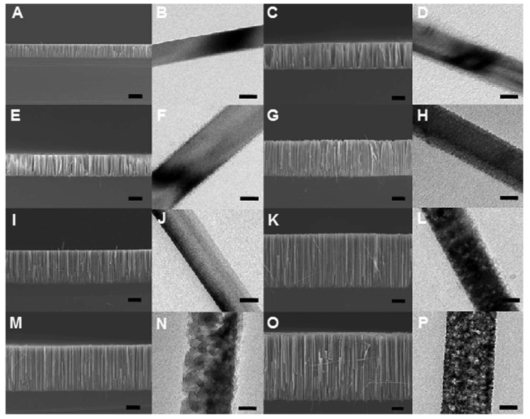
Scanning electron microscopy (SEM) and transmission electron microscopy (TEM) images of the as-grown silicon nanowires from the highly doped n-Si (100) wafers with different concentrations of H2O2 are summarized in Figure 1. For 0.1 M H2O2, nonporous nanowires were obtained as shown in TEM images Figure 1B and 1D for 30 min and 60 min, respectively. With increasing the concentration of H2O2, the silicon nanowires first become increasingly rough on the surface, and then start to evolve porous shells surrounding the solid cores, and eventually form entirely porous nanowires. For the 30 minute reaction, starting from H2O2 of 0.1M to 0.15 M, 0.2 M and 0.3M, the resulting nanowire evolve from pure solid nanowires (Fig. 1B) to rough surfaced nanowires (Fig. 1F), solid/porous core/shell nanowires (Fig. 1J) and porous nanowires (Fig. 1N). For the 60 minute reaction, the resulted nanowires follow the same trend only with thicker porous layer for the respective reactions. These studies clearly demonstrate that the increase portion of the nanowires become porous with the increase of the H2O2 concentration and reaction time.
Figure 1.
SEM and TEM images show the evolution of silicon nanowire morphology from n-Si(100) with 0.008–0.02 Ω·cm resistivity in etchant solutions composed of 4.8 M HF and variable concentrations of H2O2 through a two-step reaction. (A) and (B): 0.1 M H2O2 for 30 min; (C) and (D): 0.1 M H2O2 for 60 min; (E) and (F): 0.15 M H2O2 for 30 min; (G) and (H): 0.15 M H2O2 for 60 min; (I) and (J): 0.2 M H2O2 for 30 min; (K) and (L): 0.2 M H2O2 for 60 min; (M) and (N): 0.3 M H2O2 for 30 min; and (O) and (P): 0.3 M H2O2 for 60 min. The scale bars for all SEM and TEM images is 10 µm and 60 nm, respectively.
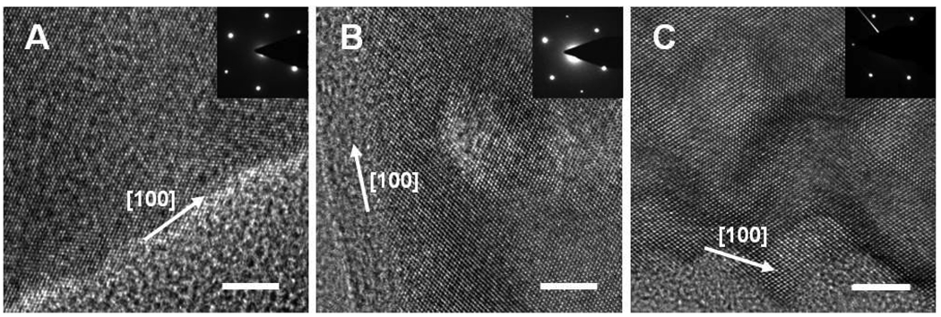
Figure 2 shows high resolution TEM images and selected area electron diffraction (SEAD, inset) patterns from as-grown silicon nanowires with 0.1 M H2O2 for 30 min, 0.2 M H2O2 for 30 min, and 0.3 M H2O2 for 60 min, respectively. The continuous lattice fringes and the single crystal-like diffraction pattern are observed in all samples, demonstrating that both the nonporous and nanoporous silicon nanowires retain the single crystalline structure of the starting silicon wafer. These studies indicate that the etching process did not destroy the crystalline integrity of the structure.
Figure 2.
(A) High resolution TEM images with SEAD patterns of nonporous and porous silicon nanowires. (A) Nanowires obtained from the reaction in 0.1 M H2O2 and 4.8 M HF for 30 min; (B) Nanowires obtained from the reaction in 0.2 M H2O2 and 4.8 M HF for 30 min; and (C) Nanowires obtained from the reaction in 0.3 M H2O2 and 4.8 M HF for 60 min. All the scale bars are 5 nm.
There is substantial difference in our etching process compared to the recent online publication34 on mesoporous silicon nanowires, including different types of starting wafers and different types of oxidant used. In the recent online publication, the formation of porosity is facilitated by the continuous reduction of silver ions in the solution.34 AgNO3 plays two roles: one is to form silver particles as catalysts and another is to work as the oxidant. In our growth, the catalysts, silver nanoparticles, are pre-deposited on the clean silicon surface. With the dissolving of silicon, electrons are transferred to silver nanoparticles to reduce H2O2 on the surface of metal particles facing to the electrolyte. Meanwhile, the metal particles etch nanopits down into the wafer. Such an electron cycle results in the formation of silicon nanowire arrays. The possible chemical reactions during the etching process are listed as the following:
Cathode (Ag surface facing to the electrolyte)
| (1) |
Anode
| (2) |
| (3) |
The total reaction
| (4) |
For the total reaction, the standard potential is 2.69 V, meaning that the etching reaction is highly thermodynamically favored. Based on our experimental results, the concentration of H2O2 is the key factor to tune the morphology of as-grown silicon nanostructures. The potential for the total reaction can be expressed as the equation 5:
| (5) |
With the increase of the of H2O2 concentration, the potential for the etching process also increases. Therefore, the driving force for the etching process becomes larger and thus increases the etching rate. The cross sections of the nanowire samples etched for the 30 min reactions show the increasing lengths with increasing H2O2 concentrations (lengths of 11.3 µm, 18.1 µm, 27.1 µm, 36.3 µm for H2O2 concentration of 0.1 M, 0.15 M, 0.2 M and 0.3 M, respectively) (Figure. 1). The same trend was also observed for 60 min etching. This phenomenon was also observed for the etching growth of silicon nanowires on p-type Si (100) and Si (111) wafers and low doped n-type Si (100) and Si (111) wafers.26
Our results indicate that the increase of H2O2 concentration can result in increasingly rough surface and eventually porous nanowires. Since H2O2 itself cannot etch the silicon off, the formation of porous structures should by facilitated by the metal nanoparticles. Previous studies suggest that the silver nanoparticles could be oxidized into silver ion during the etching process.26 In a typical etch process, the silver particles is partially oxidized by H2O2 to create a localized Ag+ ion cloud in the close proximity of the silver nanoparticles. These silver ions can quickly react with silicon and take electrons from silicon near the Ag/Si interface and be recovered into original silver particles again. In this way, the etching is localized around the silver nanoparticles and sthe ilver nanoparticles are trapped in the nanopits created by themselves, leading to continued etching in the vertical direction and the formation of vertical silicon nanowire array. However, as the H2O2 concentration increases, the concentration of Ag+ ion increases. In this case, the Ag+ ions may not be 100% recovered into the original silver nanoparticles, with some of which may diffuse out. When the amount of the out-diffused Ag+ ions reach a certain threshold, these silver ions may start to nucleate on the side wall near certain weak defective sites (e.g. around the dopants) by extracting electrons from the silicon nanowires and forming new silver nanoparticles for a new etching pathway along the lateral direction of the nanowires. In this way, the increase of H2O2 concentration increases the amount of free Ag+, and the increase of doping concentration increases the amount of weak defective points in the silicon lattice, both are important factors for the initiation of additional etching pathway in addition to the vertical etch, which explains the observation of the increased porosity with increasing H2O2 concentration during the etching of highly doped n-Si wafers.
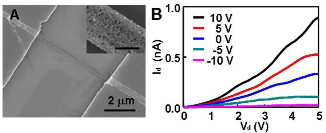
To investigate the electronic properties of the resulting porous silicon nanowies, we have carried out electrical transport studies on individual nanowires using a simple back-gated device configuration on a silicon substrate, where an underlying silicon was used as the back gate, 100 nm thick silicon nitride (SiNx) as the gate dielectric, and Ti/Au (100nm/50nm) film deposited using an e-beam evaporator as the source and drain electrodes. To fabricate the device, porous silicon nanowires were deposited onto SiNx/Si substrate, and then electron-beam lithography followed by metallization was used to define source and drain electrodes (Figure 3A). Electrical characterizations were carried out in ambient conditions at room temperature. Figure 3B shows a typical set of drain current versus drain bias voltage (Id-Vd) relations at various gate voltages (Vg) in steps of 5 V for a porous silicon nanowire device. These electrical characterization shows that the channel conductance increases with applying positive gate voltages and decreases with negative gate voltages, suggesting an n-channel transistor behavior, which is consistent with that doping type of the starting wafer. However, the overall resistance is rather larger compared to a solid silicon nanowire of similar dimension and starting doping concentration. The greatly reduced conductance can be attributed several factors: (1) the reduced current conducting volume due to the formation of porous structure; (2) the existence of a large amount of surfaces may lead to significant surface depletion of charge carriers; (3) the etching typically preferentially remove the dopants which can reduce the overall doping concentration considering the critical dimension in the porous nanowire is only around 5 nm or less; and (4) the increase of effective band gap due to quantum confinement and non-ideal source drain contact.
Figure 3.
(A) SEM image of a porous silicon nanowire device. The inset shows a higher resolution SEM image highlighting the porous structure. The scale bar in inset is 100 nm. (B) Drain current (Id) versus drain voltage (Vd) at variable gate voltages.
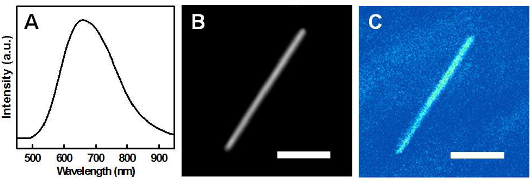
It is well known that the porous silicon can exhibit visible photoluminescence. To this end, we have also carried out studies to probe the optical properties of the resulting porous silicon nanowires in bulk solution and in individual nanowires dispersed on glass substrate. For bulk photoluminescence studies, the nanowires were released and dispersed into de-ionized water through sonication. The porous silicon nanowires can be well dispersed in the deionized water without obvious precipitation. The photoluminescence of the porous nanowires was collected from the aqueous solution under the excitation of a 473 nm laser beam from a diode laser. Importantly, the photoluminescence studies clearly show a broad visible emission centered 650 nm (Figure 4A). These studies are consistent with previous reports on porous silicon and mesoporous p-type silicon nanowires.21,34 The visible emission may be originated from the deep quantum confinement in the porous structure, and the broad emission may be attributed to broad size distribution of the critical dimension in the porous silicon nanowire structure. The optical properties of the porous silicon nanowires were also confirmed by confocal microscopy study on individual nanowires excited at 453 nm (Leica SP2 MP-FILM). For confocal studies on individual nanowires, the sample was prepared by naturally drying drops of the porous silicon nanowires solution on a glass slide. The optical micrograph of a selected single porous wire is shown in Figure 4B. The corresponding fluorescence image (Figure 4C) overlaps with the optical microscopy image, confirming the photoluminescence is indeed originated from the porous silicon nanowires.
Figure 4.
(A) Photoluminescence spectrum of porous silicon nanowires obtained with 60 min etching in a solution with 0.30 M H2O2; (B) Optical micrograph of a single porous silicon nanowires; and (C) Confocal photoluminescence image of the same single porous silicon nanowire. The scale bar in (B) and (C) is 3 µm.
In conclusion, we have demonstrated the synthesis of n-type porous silicon nanowires with single crystalline structure through a two-step reaction. We find the concentration of H2O2 is the key factor determining the rough surfaces or porous structures of the silicon nanowires. Electrical transport measurement shows that these nanowires are conductive and optical studies indicate that they can exhibit visible luminescence. The combination of electrical and optical properties in such a porous silicon nanowire may open new opportunities for nanoscale optoelectronic devices, solar energy harvesting and conversion and sensors.
Supplementary Material
Acknowledgment
We acknowledge support by the NIH Director’s New Innovator Award Program, part of the NIH Roadmap for Medical Research, through grant number 1DP2OD004342-01. We acknowledge Electron Imaging Center for Nanomachines (EICN) at UCLA for the support of TEM, Nanoelectronics Research Facility at UCLA for support of device fabrication. Confocal laser scanning microscopy was performed at the CNSI Advanced Light Microscopy/Spectroscopy Shared Resource Facility at UCLA, supported with funding from NIH-NCRR shared resources grant (CJX1-443835-WS-29646) and NSF Major Research Instrumentation grant (CHE-0722519).
References
- 1.Lieber CM, Wang ZL. MRS Bulletin. 2007;32:99–104. [Google Scholar]
- 2.Patolsky F, Lieber CM. Mater. Today. 2005;8:20–28. [Google Scholar]
- 3.Pavesi L, Dal Negro L, Mazzoleni C, Franzò G, Priolo F. Nature. 2000;408:440–444. doi: 10.1038/35044012. [DOI] [PubMed] [Google Scholar]
- 4.Li Y, Qian F, Xiang J, Lieber CM. Mater. Today. 2006;9:18–27. [Google Scholar]
- 5.Yang PD. Dalton Trans. 2008;33:4387–4391. doi: 10.1039/b801440j. [DOI] [PubMed] [Google Scholar]
- 6.Cui Y, Duan X, Hu J, Lieber CM. J. Phys. Chem. B. 2000;104:5213–5216. [Google Scholar]
- 7.Huang Y, Duan XF, Cui Y, Lauhon LJ, Kim KH, Lieber CM. Science. 2001;294:1313–1317. doi: 10.1126/science.1066192. [DOI] [PubMed] [Google Scholar]
- 8.McAlpine MC, Friedman RS, Jin S, Lin KH, Wang WU, Lieber CM. Nano. Lett. 2003;3:1531–1535. [Google Scholar]
- 9.Duan X. MRS Bull. 2007;32:134–141. [Google Scholar]
- 10.Duan X. IEEE Trans. on Electron Dev. 2008;55:3056–3062. [Google Scholar]
- 11.Javey A, Nam S, Friedman RS, Yan H, Lieber CM. Nano Lett. 2007;7:773–777. doi: 10.1021/nl063056l. [DOI] [PubMed] [Google Scholar]
- 12.Hochbaum AI, Chen R, Delgado RD, Liang W, Garnett EC, Najarian M, Majumdar A, Yang D. Nature. 2008;451:163–168. doi: 10.1038/nature06381. [DOI] [PubMed] [Google Scholar]
- 13.Tian B, Zheng X, Kempa TJ, Fang Y, Yu N, Huang J, Lieber CM. Nature. 2007;449:885–890. doi: 10.1038/nature06181. [DOI] [PubMed] [Google Scholar]
- 14.Hwang Y, Bukai A, Yang P. Nano. Lett. 2009;9:410–415. doi: 10.1021/nl8032763. [DOI] [PubMed] [Google Scholar]
- 15.Garnett EC, Yang P. J. Am. Chem. Soc. 2008;130:9224–9225. doi: 10.1021/ja8032907. [DOI] [PubMed] [Google Scholar]
- 16.Chan CK, Peng H, Liu G, McIlwrath K, Zhang X, Huggins RA, Cui Y. Nature Nanotech. 2008;3:31–35. doi: 10.1038/nnano.2007.411. [DOI] [PubMed] [Google Scholar]
- 17.Zheng G, Patolsky F, Cui Y, Wang WU, Lieber CM. Nat. Biotechnol. 2005;23:1294–1301. doi: 10.1038/nbt1138. [DOI] [PubMed] [Google Scholar]
- 18.Patolsky F, Timko BP, Yu G, Fang Y, Greytak AB, Zheng G, Lieber CM. Science. 2006;313:1100–1104. doi: 10.1126/science.1128640. [DOI] [PubMed] [Google Scholar]
- 19.Yang C, Barrelet CJ, Capasso F, Lieber CM. Nano Lett. 2006;6:2929–2934. doi: 10.1021/nl062314b. [DOI] [PubMed] [Google Scholar]
- 20.Canham LT. Appl. Phys. Lett. 1990;57:1046–1048. [Google Scholar]
- 21.Cullis AG, Canham LT, Calcott PDJ. J. Appl. Phys. 1997;82:909–965. [Google Scholar]
- 22.Lin VSY, Motesharei K, Dancil KPS, Sailor MJ, Ghadiri MR. Science. 1997;278:840–843. doi: 10.1126/science.278.5339.840. [DOI] [PubMed] [Google Scholar]
- 23.Archer RJ. J. Phys. Chem. Solids. 1960;14:104–110. [Google Scholar]
- 24.Li X, Bohn PW. Appl. Phys. Lett. 2000;77:2572–2574. [Google Scholar]
- 25.Peng KQ, Yan YJ, Gao SP, Zhu J. Adv. Mater. 2002;14:1164–1167. [Google Scholar]
- 26.Zhang ML, Peng KQ, Fan X, Jie JS, Zhang RQ, Lee ST, Wong NB. J. Phys. Chem. C. 2008;112:4444–4450. [Google Scholar]
- 27.Peng KQ, Xu Y, Wu Y, Yan YJ, Lee ST, Zhu J. Small. 2005;1:1062–1067. doi: 10.1002/smll.200500137. [DOI] [PubMed] [Google Scholar]
- 28.Peng KQ, Zhu JJ. Electroanalytical Chem. 2003;558:35–39. [Google Scholar]
- 29.Peng KQ, Hu JJ, Yan YJ, Wu Y, Fang H, Xu Y, Lee ST, Zhu J. Adv. Funct. Mater. 2006;16:387–394. [Google Scholar]
- 30.Peng KQ, Fang H, Hu JJ, Wu Y, Zhu J, Yan YJ, Lee ST. Chem. Eur. J. 2006:7942–7947. doi: 10.1002/chem.200600032. [DOI] [PubMed] [Google Scholar]
- 31.Huang ZP, Fang H, Zhu J. Adv. Mater. 2007;19:744–748. [Google Scholar]
- 32.Huang ZP, Shimizu T, Senz S, Zhang Z, Zhang XX, Lee W, Geyer N, Gösele U. Nano. Lett. 2009;9:2519–2525. doi: 10.1021/nl803558n. [DOI] [PubMed] [Google Scholar]
- 33.Peng KQ, Zhang ML, Lu AJ, Wong NB, Zhang RQ, Lee ST. Appl. Phys. Lett. 2007;90:163123. [Google Scholar]
- 34.Hochbaum AI, Gargas D, Hwang YJ, Yang P. Nano. Lett. 2009 doi: 10.1021/nl9017594. online, DOI: 10.1021/NL9017594. [DOI] [PubMed] [Google Scholar]
Associated Data
This section collects any data citations, data availability statements, or supplementary materials included in this article.


