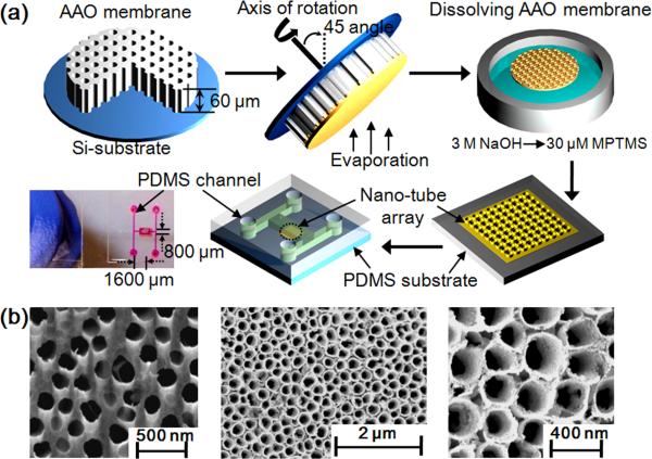
Fig. 1.
(a) Schematic of the SERS active nanotube array fabrication procedure. Anodized alumina (AAO) membrane is attached onto a silicon substrate. After mounting AAO substrate on a rotating chuck, the desired metal structure is deposited onto membrane with an incident 45° angle to the axis of rotation. The metal deposited membrane is then soaked in 3.0 M NaOH for 10 min to dissolve the AAO shadow membrane and yield a metallic nanotube array connected by a continuous backing of the deposited material. After dissolution, the array is dipped in a 30 μM MPTMS solution for 2 hr as an organic adhesion layer aiding with the transfer of the nanotube arrays to the PDMS substrate. The enclosed optofluidic chip was then assembled by bonding that substrate with an upper PDMS microfluidic structure fabricated using traditional soft-lithography techniques. Final device dimensions are 0.8 (width) × 1.6 (length) mm. (b) SEM images of (1) bare AAO membrane and (2, 3) nanotube arrays after dissolving the AAO shadow membrane. The nanotubes formed after evaporation of Au/Ag/Au at an incident angle 45° are about 200 nm diameter and 200 nm height.

