
Fig. 2.
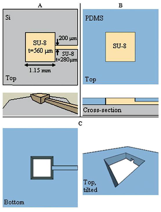
Fabrication of a fluidic layer. (A) A two-layer SU-8 structure is patterned onto a Si wafer. (B) PDMS is poured onto the mold so that it entirely covers the channel, and the taller SU-8 post creates a through-hole in the PDMS. (C) After curing, the PDMS can be peeled off of the mold to yield the structure shown here.