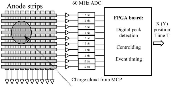
Fig. 2.

Schematic diagram of the parallel cross strip data processing electronics. Each electrode of the two orthogonal set of fingers is connected to a charge sensitive preamplifier followed by a fast ADC. All digitized channels are fed into Vertex5 FPGA, where an event is detected, peak values are calculated for the electrodes which received charge from MCP cloud followed by the event centroid calculation. The same data is used for calculation of the event timing. Only one set of fingers has its electronics shown.
