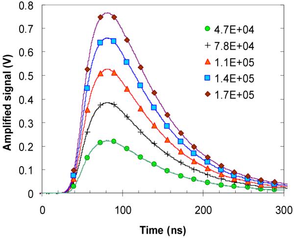
Fig. 3.

The measured shape of the signals from the charge sensitive multichannel preamplifier board with RD20 ASIC followed by single stage postamplifiers to match the ADC input dynamic range. Signals from only one channel are shown, the others are identical with exception of the pedestal offset, which is corrected in the FPGA data processing. The legend shows the values of the input charges in number of electrons. Solid lines – measured by a 500 MHz digital scope, markers – the values digitized by a 60 MHz ADC.
