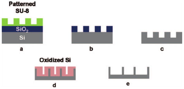
Fig. 3.

Fabrication process of the Si mold for nanoimprint process: (a) imprinted SU-8, (b) transfer of pattern to SiO2 by fluorine ICP etch, (c) transfer of pattern to Si by chlorine ICP etch; (d) repeated oxidation and oxide removal by BOE, and (e) final Si mold.
