Fig. 4.

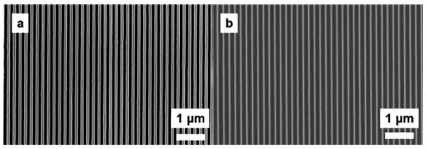
SEM micrographs showing (a) the Si grating after the second oxidation and oxide etch step and (b) the final Si grating (after all oxidation and oxide etch steps) with ∼20 nm wide Si lines that is used to make the nanoslots.

SEM micrographs showing (a) the Si grating after the second oxidation and oxide etch step and (b) the final Si grating (after all oxidation and oxide etch steps) with ∼20 nm wide Si lines that is used to make the nanoslots.