
Fig. 1.
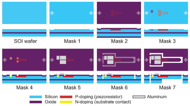
Piezoresistive cantilever fabrication process. (Mask 1) Pattern alignment marks. (Mask 2) Grow 250-Å screening wet oxide at 850 °C for 13 min, and pattern piezoresistors; then, ion implant 2 · 1014, 2 · 1015, 5 · 1015, and 1016-cm−2 boron for the piezoresistor regions. (Mask 3) Pattern n++ region, and ion implant 5 · 1015-cm−2 arsenic for substrate contact; then, etch damaged oxide in 6 : 1 buffered oxide etch (BOE). (Mask 4) Grow isolation wet oxide at 1000 °C– 1150 °C (15–45 min) plus 1000 °C–1150 °C inert N2 anneal (5–32 min); then, pattern and wet etch (6 : 1 BOE) contact vias through the oxide. (Mask 5) Sputter 1 μm of 99% Al/1% Si; then, pattern and wet etch (Olin Aluminum Etch II) the Al. (Mask 6) Pattern cantilevers, and etch the oxide and silicon with 6:1 BOE, then deep reactive ion etch (DRIE) stopping on the buried oxide layer. (Mask 7) Leave front-side resist, and release the cantilevers using back-side pattern alignment, then a DRIE process stopping on the buried oxide again; remove buried oxide from cantilevers using RIE, and finally anneal the wafers in H2 forming gas at 475 °C (10 min) to improve contact resistance and noise.