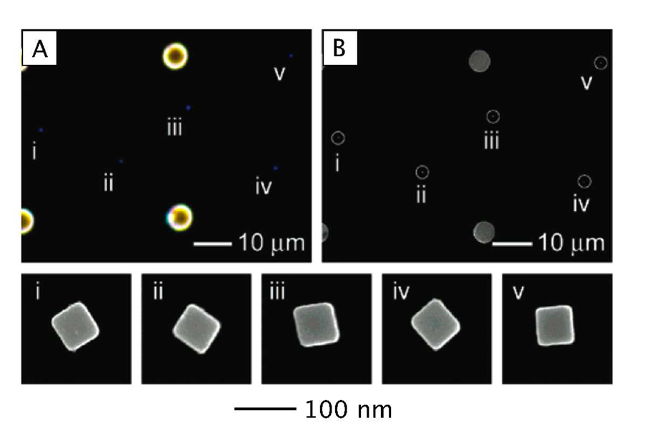
Figure 3.
(A) Dark-field optical micrograph of a Si substrate with registration marks (large yellow spots) and a number of individual silver nanocubes (small blue dots) labeled i to v; and (B) SEM image of the same region as shown in (A). Below (A) and (B) are the SEM images clearly resolving the morphology and orientation of each individual nanocube. Copyright (2007) ACS.

