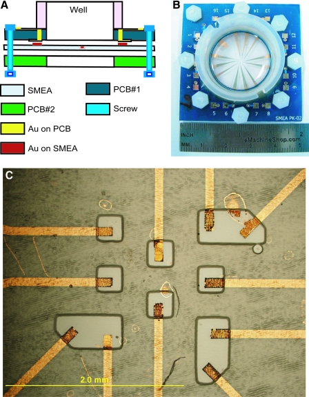
FIG. 1.
Schematic and image of the SMEA package. (A) After fabrication, the SMEA was clamped between two printed circuit boards (PCB) to form an interface between it and the amplifier. A plastic well was cemented onto the top PCB to form a tissue culture chamber. (B) Image of a packaged SMEA. The 49 mm × 49 mm sandwich of PCB-SMEA-PCB was used as an interface with the MCS multichannel amplifier for recording and stimulation. (C) Image of the 11-electrode array in the center of the SMEA. The tips (100 μm × 200 μm) of the patterned conductors were exposed by photopatterned vias in the encapsulation layer to form 11 independent recording electrodes and were modified by platinum black to reduce electrode impedance. (Color image may be found on our website at www.liebertpub.com/jon)

