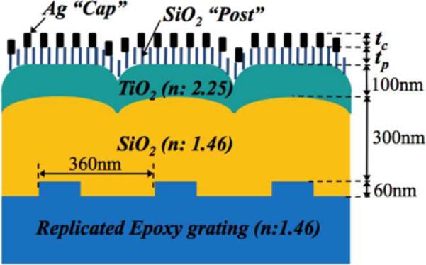
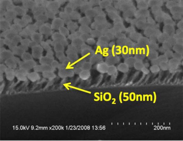
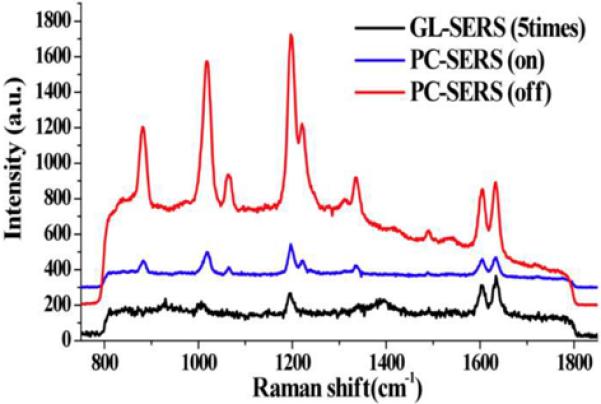
Figure 8.


a). Cross section schematic of the PC surface structure used for PC-SERS. The PC surface is covered with a layer of dielectric nanorod “posts” that each support a 20–30 nm diameter Ag “cap” for obtaining the SERS effect. The design goal is for the Ag caps to reside within the evanescent field region of the PC when it is illuminated with a laser at a combination of wavelength and incident angle that excites an optical resonance. b). Scanning electron microscope photo of the post-cap structures, c). Measured SERS signals from a layer of BPE, comparing the SERS intensity with the post-cap structures without a PC (GL-SERS curve), with a PC illuminated at an angle that does not excite resonance (PC-SERS (off)) and at an angle that excites resonance (PC-SERS (on)). (Reprinted with permission from the American Physical Society, Appl. Phys. Lett., Vol. 93, p. 143122,2008.)
