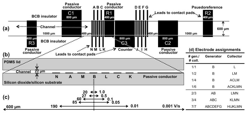
Figure 1.
Design, dimensions, and labeling schemes of elements on the microelectrode array/channel chip. (a) Top-down schematic shows electrode-containing region of the chip. Active electrode lengths and channel width are defined by the 600-μm wide opening in the overlying BCB insulator layer and indicated by the two, thin horizontal lines. Microband array electrodes, A through N, are each 50-μm wide. All unlabeled gaps are 25-μm wide. (b) Lengthwise, cross-section schematic shows an expanded side-view region of the array with a 22-μm high microchannel when the PDMS lid is on. (c) Estimated diffusion lengths, δ (μm), measured specifically here from the “B” electrode for different timescales (represented by different scan rates, V/s). (d) Table lists generator and collector electrodes used during redox cycling experiments. All features within each image are drawn to-scale with the exception of the electrode heights in part (b) (100. nm gold plus a 7.5 nm chromium adhesion layer), which would otherwise be too thin to see in the diagram, and the thickness of the substrate and PDMS lid in part (b).

