Abstract
We report on the development of an inexpensive, portable lab-on-a-chip flow cytometer system in which microfluidics, photonics, and acoustics are integrated together to work synergistically. The system relies on fluid-filled two-dimensional on-chip photonic components such as lenses, apertures, and slab waveguides to allow for illumination laser beam shaping, light scattering and fluorescence signal detection. Both scattered and fluorescent lights are detected by photodetectors after being collected and guided by the on-chip optics components (e.g. lenses and waveguides). The detected light signal is imported and amplified in real time and triggers the piezoelectric actuator so that the targeted samples are directed into desired reservoir for subsequent advanced analysis. The real-time, closed-loop control system is developed with field-programmable-gate-array (FPGA) implementation. The system enables high-throughput (1–10kHz operation), high reliability and low-powered (<1mW) fluorescence activated cell sorting (FACS) on a chip. The microfabricated flow cytometer can potentially be used as a portable, inexpensive point-of-care device in resource poor environments.
Keywords: Microfluidics, Photonics, Sensor, On-chip optics, Flow Cytometry, FACS
1. INTRODUCTION
Microfluidics is an emerging technology that manipulates small volumes of fluid (e.g. nanoliters to picoliters), by using of microchannels with dimensions of hundreds of micrometers or smaller. Over the past decades, the field of microfluidics has evolved to encompass a wide range of applications, such as fluid mixing [1], pumping liquids [2], cell culturing [3] and much more. Owing to the small microchannel dimensions, the fluidic system has a low Reynolds number, thus controlled laminar flow systems are easily achieved. Microfluidic devices are also small and portable. After soft lithography techniques and PDMS replica molding processes were developed [4], microfluidics gained an inexpensive platform for rapid prototyping so that fabrication cost and time have been significantly reduced to show the possibility of mass production. There have been huge efforts to expand functionalities into different research areas by integrating other fields like electronics, optics, and acoustics with microfluidic systems on a chip. Recently, photonics has come to be integrated onto microfluidic chips in a new field referred to as ‘optofluidics’, in which ‘microfluidic photonic integrated circuits’ are formed [5]. In microfluidic photonic integrated circuits, photonics and microfluidics are synergistically combined to create novel functionalities. Unlike solid materials, the optical properties of the optofluidics system can be reconfigurable by simply replacing the fluid of flowing streams inside the device. With its potential for highly integrated reconfigurable lab-on-a-chip devices, the microfluidic photonic integrated circuit can revolutionize the fields of biology, chemistry, biomedicine and more.
The flow cytometry system on a chip finds some of its best applications in the field of biomedicine. The flow cytometer is a widely used bench-top device for identifying subpopulations within a sample of cells. Cells flow rapidly in a controlled fashion through a narrow laser beam of the interrogation region. When cells pass through the interrogation region, both scattered and fluorescent light from the cells are measured by built-in on-chip optic components and photodetectors (e.g. PMT). Multi-angle scattering light measurements reveal morphological information, while detecting fluorescence emitted from fluorescent tags gives further insight into cellular identity [6]. Reagents with different fluorescence spectra can be used to simultaneously tag and measure multiple parameters for every single cell in the sample, giving a wealth of information in a single cytometer run. This conceptually simple scheme has broad applicability, from routine blood work to the diagnosis and monitoring of diseases like HIV or Leukemia. While these methods are accurate, the bench top flow cytometer is very expensive ($100,000) and bulky (e.g. non-portable) and it further requires a trained operator and a large volume of sample. Therefore, there has been a need to develop smaller, less expensive and potentially portable flow cytometers that operate on small sample volumes for more widespread laboratory and clinical use [7].
In this paper, we introduce a lab-on-a-chip flow cytometry system which is small, inexpensive and portable. It requires only a small volume of sample due to its micrometer-sized channel dimensions. In keeping with our goal of developing a low cost, highly functional portable flow cytometer, we employ small, low-powered components to the system. The microfluidic flow cytometer specifically explores the utility of a fluid-filled on-chip optical system for highly sensitive detection and the implementation of a real-time sorting system using a low-powered piezoelectric-based actuator for high-throughput, accurate sorting of targeted cells.
For the optical detection portion of the device, several optofluidics techniques are combined to improve light collection efficiency and enable multi-channel analysis while maintaining a low fabrication cost. The main features of the optical detection system are fluid filled slab-waveguides and two-dimensional (2D) fluid filled lenses. All of these optical components are easily reconfigurable (by replacing fluids) and highly integrated. They are precisely aligned on a compact, easy-to-fabricate chip. The integration of optical components onto the chip offers an advantage over off-chip optics: the system is capable of generating a wide range of on-chip lens curvatures that could become prohibitively expensive when fabricated off-chip. For example, a wide range of aspherical lens profiles (nearly any profile desired) can be created. The ability to create custom lenses, waveguides, apertures and other optical elements expands the ‘optical toolbox’ available to microfluidic devices. Combined with proper system design, the development of highly sensitive optofluidic devices is becoming a reality.
With the information obtained from the 2D optical detection system upstream, the real-time sorting of targeted samples is performed downstream in the microfluidic flow cytometer. A piezoelectric actuator is integrated on a chip to electronically manipulate flow streams based on a pushing and pulling mechanism. As the piezoelectric disc bends and displaces fluid stream, particles entering the sorting junction will be deflected to the appropriate collection channel. The direction and extent of fluid deflection can be easily manipulated by adjusting the applied voltage of this low powered (<1mW) system. The fast actuation and the closed-loop real-time FPGA control system enable our microfluidic flow cytometer to sort many cells (at least ~1000 cells/sec) rapidly and precisely with high purity.
2. EXPERIMENTAL
2.1 Overview
Our microfabricated flow cytometer is a PDMS-based on-chip device comprised of a fluidic system for sample flow and an optical system for sample illumination and interrogation. Introduced light travels in the core region (n_core=1.46) of a higher refractive index PDMS slab waveguide, which is cladded by two thicker PDMS regions (n_cladding=1.41) with lower refractive index by total internal reflection (TIR). Prisms and lenses on a chip are filled with optical fluids or elastomers which have a higher refractive index and the necessary dispersion properties. Once the optical elements have been completely filled, elastomers can be cured, creating a robust chip that is easy to handle. Waveguides and lenses shape incoming light to illuminate the sample, and scattered and fluorescence lights are similarly collected by on-chip 2D lenses and guided by slab waveguides until reaching photo-detectors. Detected signal is imported and amplified using the real time processing system built with Compact RIO module (National Instruments). The amplified signal output triggers the PZT actuator to deflect so that targeted samples are directed to the desired sorting channel.
2.2 Device Fabrication
2.2.2 Optical System Fabrication/Structure
Our lab-on-a-chip flow cytometer was fabricated by soft lithography (mold-replica) techniques [4]. Molds are made by one of two microfabrication processes. In the first, standard UV lithography techniques are used to transfer a pattern from a photomask into roughly 50μm of SU-8 50 (Microchem) negative photoresist on a Si wafer. After development of the photoresist, the remaining SU-8 on the Si substrate forms the device features of the mold, such as fluidic channels, two-dimensional lenses, prisms, etc. Subsequent hard baking for 1hr at 200°C improves robustness of the mold.
The second, newer process is a cryogenic etching process used to create all-silicon mold masters. These molds are more robust, and the cryogenic process also delivers more vertical sidewalls with a low surface roughness, which can be even further reduced via post-processing techniques such as wet etching. In the cryogenic process, an inductively-coupled plasma (ICP) etcher (Oxford PlasmalabSystem 100) is operated at cryogenic temperatures (e.g. −115°C) using oxygen and SF6 gases to simultaneously etch the silicon mold while passivating the sidewalls to prevent further etching. With the mold fabricated, PDMS replicas are easily produced. The master molds are dessicated in a vacuum with (tridecafluoro-1,1,2,2,-tetrahydrooctyl)-tricholosilane (United Chemical Technologies) to create a hydrophobic layer on the surface for easier demolding. PDMS prepolymer (Sylgard 184, Dowcorning) mixed with curing agent at 1:10 ratio was poured onto the mold and cured for 2hrs at 65 °C. For the molded side of the device, the core layer consists of a spin-coated high index polymer (Nusil LS-6946). The cladding layer, poured directly on top of the newly-spun core layer, is a lower index PDMS (Gelest OE41). A blank wafer serves as a second ‘mold’ to create the capping layer, consisting again of poured low-index polymer (Gelest OE41) to serve as cladding on the other side of the core layer. Both replicas are cured for 3–6 hours at 65°C.
For both the sorting and optical detection portions of the device, the PDMS layers are peeled off of the molds after curing. Holes for any sample inlets/outlets, two-dimensional photonic components and/or actuation chambers are then punched, and all PDMS surfaces were UV/Ozone treated to facilitate strong covalent bonding between the top and the bottom layer. Optical fibers have been used to interface between the device waveguides and the external laser source and Si photo-detectors (Thorlabs). 50/125 μm fiber (Corning) was inserted into a fiber sleeve in the device, which aligns the fiber to internal cladding waveguides. On-chip waveguides are finished by using capillary action to fill the cladding channels with a low index PDMS (Gelest OE41) and curing at 65°C for 2–4 hours. Some devices have also been directly interfaced using a fiber coupled laser. In this setup, a fiber tip is directly aligned to the polymer waveguide facet. On-chip lenses are filled with a high index fluid (LS-5257) or a partially-cured high index elastomer (LS-6257), which is subsequently cured at 150°C for up to one hour.
2.2.2 Sorting System Fabrication/Structure
The sorting system, based on a piezoelectric actuator, was built as shown in Figure 1. A bimorphous piezoelectric/metal disc made of Lead Zirconate Titanate (PZT) and stainless steel is integrated on a PDMS chip to manipulate flow streams based on a “push-pull” mechanism. The PZT disc has a diameter of 20mm and a resonant frequency of 5 kHz under ‘load-free’ conditions. As the PZT actuator bends downward and pushes on the flowing fluid, the samples entering the sorting junction will be deflected to the left collection channel. In contrast, during the steady-state of the PZT disc, a sample will travel straight down passing the sorting junction into the center waste channel.
Fig. 1.
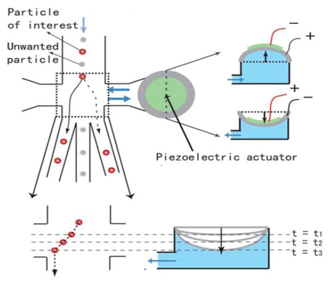
Operating principle of the PZT actuated sorting system. Bending of the PZT disc temporarily disturbs fluid flow so that particles are deflected to the left or the right sorting channels. The amount and the direction of bending of the PZT actuator are electronically controlled by the polarity and the magnitude of the input voltage.
A PZT actuator is integrated with the actuation chamber of the PDMS chip using UV/Ozone surface treatment, as discussed earlier. The strong bonding between the PZT and the PDMS chip has the advantages of preventing fluid leakage and enabling efficient coupling of the PZT actuator to the fluidic chamber for low-powered (<1 mW) operation [8].
A control algorithm is implemented in FPGA to perform the following tasks in real time: signal processing to enhance the signal-to-noise ratio, deciding whether the detected sample is to be sorted, creating a time delay matching the propagation time from the detection zone to the sorting junction, and producing a voltage signal of the specified waveform and amplitude to drive the piezoelectric actuator. This closed-loop system to carry out detection and sorting produces a timing jitter of less than 10 μsec, suggesting a potential throughput of the order of 100,000 samples/sec compared favorably to the state-of-the-art FACS systems. Our real time, closed-loop control system is programmed using LabVIEW (National Instruments) with an external driver (Compact RIO, National Instruments) that has an independent operating system with an embedded field-programmable-gate-array (FGPA) chip.
3. RESULT AND DISCUSSION
3.1 Optical Detection
Our previous work has shown the development of a method of creating two-dimensional lenses in the plane of a microfluidic channel by using fluid-filled channels with curved shapes as refractive elements [9]. Our later work has shown operation of a basic microfluidic cytometry chip with integrated optics [10, 11]. In these chips, two spherical lenses were used to shape the illumination beam, and two more were used to collect light and couple it into outgoing waveguides for each detection line. Bead-based light scatter experiments showed that this proof-of-concept chip was able to count passing particles with a low (9 to 15%) scatter intensity coefficient of variation (CV). This sets the record performance in the chip-based light scattering detection device and the result is comparable to the commercial benchtop system (CV about 10%). However, this protoype version of the device is not adequate for multi-color fluorescence detection due to the oversimplified optics, which is insufficient to capture the much weaker fluorescence signals in high throughput operation. Another area for improvement is the high background level of “forward scattering” detection without a beam stop to block the direct transmission of the incident laser beam. Optical ray-tracing design tools (ZEMAX and CodeV) are applied to create some of the most sophisticated optofluidic circuits integrated with microfluidic channels to match or exceed the performance of commercial benchtop systems in these areas. The design may involve as many as 12 optical interfaces in the light path before reaching the detector. The increasing complexity of the system imposes a technology challenge in device fabrication: the quality of the interface. The interface between media of substantial index difference needs to be smooth to reduce the scattering loss. The verticality of the sidewall also needs to be within 2-degrees from a 90-degree wall. Including the Fresnel loss (typically <2% per interface), scattering loss, and deviation from a 90-degree side wall, the total loss at each optical interface should be kept below 5% (or 0.4 dB per interface). This suggests that the method of creating the mold master should be modified and the often-used SU-8 mold making method needs to be replaced with methods such as the deep-ICP etched Si mold as detailed below.
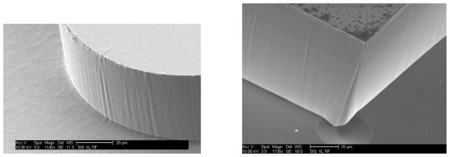
Figure 2 shows an SEM image of features in a cryogenically-etched silicon mold. Note the highly vertical sidewalls and smooth edges. Interferometric analysis (NT1100, Veeco) of small patches, for example 20 μm × 20 μm, has shown RMS sidewall roughness of ~30 nm. For an excitation wavelength of 488 nm and an average index of the medium of 1.5, the surface roughness is about 1/10 of the wavelength, yielding low scattering loss. With process optimization, the surface roughness is expected to be reduced further. In addition, we are investigating the use of wet etches to further reduce sidewall roughness.
Fig. 2.
Edge of a cryogenically-etched mold for a lens (left) and a waveguide (right). Larger scale ripple is the result of lithography problems, not limitations of the cryogenic process. The waveguide (right) still has the metal mask coating on the top along with some fragments around it, which are all removed by a wet etching process after the initial etch. Note the highly vertical sidewalls in of the lens, and the excellent smoothness of the waveguide
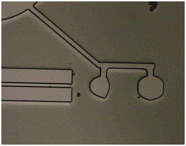
The development of a broad optical toolbox (the ability to fabricate quality elements including waveguides, lenses, and even beyond) is another key component to achieving higher system performance. We have created waveguides using a single filled channel as the waveguide core, or using two filled parallel channels as the cladding. Multimode waveguide losses have been measured at 3.5dB/cm with SU-8 mold, and are expected to drop dramatically with the recently developed Si molds. The nature of our technique for creating on-chip optics allows for the manufacturing of complex lens shapes, including parabolic and aspheric lenses, such as those shown in Figure 3.
Fig. 3.
Custom lens shapes, such as the parabolic lenses shown here, are available to designers of systems with two-dimensional in-plane optics. These lenses are made in the exact manner as simple spherical lenses, unlike their bulk counterparts which can be very labor-intensive to produce
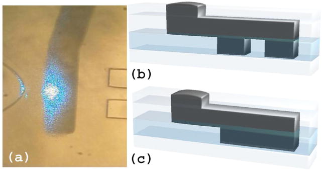
On the other hand, creating aperture stops or beam blocks require totally black material not part of the previous process. The incorporation and patterning of light absorbing materials into the optofluidic circuit requires new process development. We have identified an opaque material for beam stops and apertures. Figure 4 shows a blocking bar and a similarly-formed aperture, demonstrating the light blocking abilities of these structures. Exploiting the dispersive properties of silicone elastomers, we have also designed two-dimensional prisms for beam directing and chromatic separation. Each of these elements is important to allow freedom of design for lab-on-a-chip devices such as the microfluidic flow cytometer and also many other types of devices.
Fig. 4.
(a) Image of a beam blocking bar between a lens (left) and a waveguide (right). Apertures (b) and beam blocking bars (c) are made by filling channels in the light guiding layer (darkest region, second to bottom) via a filling channel in the capping layer (represented by the top two layers, the lower portion containing filling channels and the upper portion containing punch holes for channel access). The aperture (b) will block stray light, allowing light to pass only through the center portion. The beam blocking bar (c) is used to verify the light blocking capabilities of the filled channels.
With the above mentioned technology advancement, we are able to create a lab-on-a-chip cytometer with a sophisticated optical system. Our chip’s detection lines have locations analogous to those in a benchtop cytometer: side scatter at 90 degrees and forward scatter in the forward direction via the use of a beam stop to block laser light. Our device design includes aspherical lenses and apertures for stray light control. The illumination beam can be shaped by lenses. All of these capabilities will help to create a device with superior resolution on a miniaturized platform. An example of a prototype cytometry chip is shown in Figure 5. This ability to design sophisticated on-chip optical systems is readily transferred to a variety of other microfluidic-photonic applications, enabling a host of new, higher-quality devices to be created.
Fig. 5.
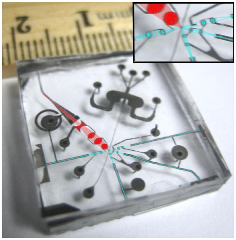
An image of a prototype of microfluidic flow cytometer, showing incoming and scattered light lines (in blue) as well as a large numerical aperture fluorescence collection line (in red). Each line has two integrated fluidic lenses that are, by fabrication, perfectly aligned to their respective waveguides and to the fluidic channel. The entire chip is very compact, measuring roughly 2 cm × 2 cm with the two-dimensional optical toolbox. Scattering detection (blue colored) and fluorescence detection (red colored) optics systems are integrated on a chip with a small form factor.
3.2 Microbeads and E-Coli Sorting
The operation principle of the push/pull mechanism is experimentally verified by introducing 5mM Rhodamine 6G solution into flow stream as shown in Figure 6. As the PZT actuator bends upward, the fluid at the sorting junction is pulled to the right channel (Figure 6(a)). When the PZT moves downward, the flow stream is pushed to the left (Figure 6(b)). When the PZT doesn’t move, samples suspended in the fluid enter the center waste channel (Figure 6(c)).
Fig. 6.
Image showing deflection of rhodamine dye as a result of PZT actuation. As the PZT surface bends upward (or downward), the rhodamine stream is switched to the right (or left) channel. When PZT actuator is turned off, flow enters the center channel without deflection. The photos were taken with a high-speed (3000 frames/s) CCD camera.
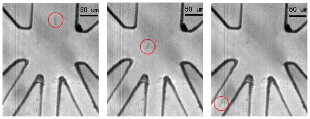
The direction and magnitude of the deflection of the PZT is controllable by the polarity, magnitude, and waveform of the applied voltage. The PZT operates under low voltage (< 10V peak-to-peak) and low-power (<1mW) and has a response time below 1ms. All these features are critical to creating an inexpensive and portable cell sorter of high throughput. A sample of 5-μm polystyrene beads at a concentration of ~ 3.2 × 10⁵ beads/ml (Bangs Lab) is introduced into to the microfluidic channel. The suspended beads, confined by the sheath flow, travel at a velocity of ~ 5 cm/sec. The PZT actuator is modulated at 250 Hz at 9 Vp-p. Experimental images (Figure 7) are obtained from videos taken at the sorting junction at 3000 frame per second (fps). The sequential images show that as the PZT actuator bends down, the particle at the sorting junction is deflected toward the left channel due to the PZT-induced drag force. Similarly, when the PZT actuator bends up, the particle is deflected toward the right channel. The result shows that the sorter can impose sufficient drag force to alter particle trajectory.
Fig. 7.
Sequential images showing particle trajectory at time 0ms, 1.3 ms and 3.3 ms. The downward bending PZT actuation creates fluid displacement, which in turn drags the particle to the left and eventually down the collection channel. The experiment is carried out under 250 Hz (e.g. sinusoidal) and 9 Vp-p PZT actuation. Sorted bead is marked by a circle.
To further characterize the sorting mechanism, an E. coli concentration of ~ 7 × 10⁵ cells/ml is prepared and suspended in 1X PBS solution. Total volumetric flow rate is maintained at 18 μl/min, and the PZT actuator is operated under 5 Vp-p and 200 Hz. Videos recorded at 6000 fps, and the sorted E. coli cells (e.g. sorted to the left and right collection channels) are enumerated using frame-by-frame images to characterize the sorting capability of the device. At this flow rate, we expect the E. coli cells to pass through the sorting junction (~100 μm in length) in 1.7 ms.
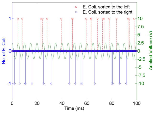
Figure 8 shows the sorting result of the aforementioned experimental conditions. Individual peaks represent single cells entering the right/left collection channels at the specified times. With frame-by-frame analysis, we determine the sorting rate to be 330 cells/sec. Notice that, without exception, all of the left (red) peaks occur within the rising slope and all of the right (blue) peaks occur within the falling slope of the applied voltage. This is consistent with our proposed sorting mechanism, since rising/falling slope signifies the PZT membrane is in the process of bending downward/upward, which in turn pushes/pulls the cells to the desired collection channel.
Fig. 8.
Sorting of single E. Coli cells at 200Hz frequency and 5 Vp-p actuation voltage. The peaks are obtained by identifying cells visually as they are sorted to the left/right collection channels. Approximately 18 and 17 E. Coli cells are sorted to the left/right in 100ms in this case. A total of 330 cells are visually counted over 1 sec. Note that the cells that are sorted to the left/right all fall into downward/upward (bending down/up) ramping state of the PZT actuator, as predicted by the theory.
The real-time closed loop control system with FPGA implementation is developed using LabVIEW cRIO module. The system imports the detected fluorescence light signal from upstream and amplifies the signal with a digital match filter. The signal amplification improves the signal-to-noise ratio (SNR) by a factor of ~18 dB. Such SNR enhancement is needed for fluorescence detection because of the low signal intensity. When the detected light intensity is higher than the user-set threshold voltage, an output voltage (<10Vp-p) is applied to the PZT actuator after certain delay time calculated by sample flow velocity. For a sample traveling at a speed of 2~5cm/sec over a sorting area that is 100μm long, it takes 2~5 ms for the targeted sample to be redirected into the sorting channel. Therefore, by setting up an appropriate delay time, the PZT actuator moves upward/downward (or stays still) to sort each sample to its destination. The system produces a timing jitter of <10 μs, enabling us to sort cells, beads, and biomolecules in real time with high accuracy.
To characterize the sorting accuracy and efficiency of the sorter, 10-μm fluorescent beads (Bangs Laboratory) with a concentration of ~ 1 × 10⁵ particles/ml and excitation/emission wavelengths of 480/520 nm are used. The beads are hydrodynamically focused under a sample-to-sheath flow ratio of 1:2. The beads travel at a velocity of ~ 8 cm/sec. Square (1.5 ms) voltage pulses of ~ 10 Vp-p are used to drive the PZT actuator. The voltage pulse has a rise and fall time of about 0.1 ms. The delay time is estimated to be 1.5 ms based on the velocity of the particle and the distance between the detection zone and the sorting junction. The data recording time is 10 seconds. For most applications, sorting accuracy is more important than sorting efficiency. The former refers to the rate of sorting error defined as the percentage of samples entering the designated channel by mistake. The latter refers to the successful rate of directing the targeted sample to the designated channel. In most cases, one would minimize the sorting errors at some expense of sorting efficiency.
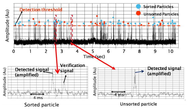
All blue dots in Figure 9 are samples successfully sorted to the designated channel, and the red dots represent samples that fail to enter the designated channel although their fluorescent signals are above threshold. The reason for missing these samples may be due to imperfect timing control or an applied voltage of insufficient magnitude. The sorting efficiency is ~70%. However, the experiment shows 0% error rate. In other words, the system does not falsely sort beads with intensity less than the threshold. One unique and attractive feature in the integrated cell sorter is the on-chip verification function. For every sample being sorted to the designated channel, a secondary fluorescent signal is detected to verify the sorting event. In consequence, each successfully sorted bead shows two consecutive peaks, one from the detection zone and the other from the verification zone (lower left of Figure 9). On the other hand, those beads that are not successfully sorted show only one peak with the verification signal missing (lower right of Figure 9). This allows us to keep track of the sorting efficiency and sorting accuracy during the experiment. In case the efficiency or accuracy drops below the acceptable value, one can immediately pause the experiment and reestablish proper operation conditions.
Fig. 9.
Sorting efficiency data. Within the time period, 44 beads out of 64 detected fluorescent beads are sorted, resulting in ~ 70% sorting efficiency. For every sorted bead, the detected signal is followed by a verification signal (lower left figure). In contrast, the absence of verification signals indicates particles that are not being sorted (lower right figure).
4. CONCLUSION
We describe an on-chip microfluidic flow cytometer and FACS system combining three key technologies in the same platform: microfluidics, photonics, and acoustics. Highly sophisticated two-dimensional optical circuits are fabricated to detect scattered and fluorescent light. The photonic circuits contain fluid-filled 2D lenses, waveguides, prisms and other elements such as beam stops and apertures. Thus an optical toolbox is essentially established based on fluid-filled integrated optics technologies. As the complexity of the optic system increases, the requirement for interface quality becomes more demanding to assure low optical loss. To meet the performance requirement, inductively-coupled-plasma etched Si molds formed under cryogenic etching condition are used to replace conventional SU-8 molds. The cell sorting system using integrated piezoelectric acoustic actuators has demonstrated several advantages for μFACS systems. While maintaining low cost and low-powered operation, the on-chip PZT actuator has fast response time (0.1–1ms) to allow for high-speed single cell sorting. The control system implemented in FPGA offers real-time SNR enhancement, user-defined delay time and output waveform, and a timing jitter of < 10 μsec. A closed-loop μFACS system based on the technology platform discussed in this paper has demonstrated a sorting efficiency of 70% and sorting-error-free operation, a major step towards the objective of portable, low cost, high performance flow cytometer and μFACS.
Acknowledgments
The authors acknowledge the technical support from the staff of the Nano3 facility in Calit2 and the financial support from NIH grant 1R21RR024453-01.
References
- 1.CHEN H, MEINERS JC. TOPOLOGIC MIXING ON A MICROFLUIDIC CHIP. APPLIED PHYSICS LETTERS. 2004;84:2193. [Google Scholar]
- 2.BEEBE DJ, MENSING GA, WALKER GM. PHYSICS AND APPLICATIONS OF MICROFLUIDICS IN BIOLOGY. ANNUAL REVIEWS IN BIOMEDICAL ENGINEERING. 2002;4:261–286. doi: 10.1146/annurev.bioeng.4.112601.125916. [DOI] [PubMed] [Google Scholar]
- 3.INOUE I, WAKAMOTO Y, MORIGUCHI H, OKANO K, YASUDA K. ON-CHIP CULTURE SYSTEM FOR OBSERVATION OF ISOLATED INDIVIDUAL CELLS. LAB ON A CHIP. 2001;1:50–55. doi: 10.1039/b103931h. [DOI] [PubMed] [Google Scholar]
- 4.XIA Y, WHITESIDES GM. SOFT LITHOGRAPHY. ANNUAL REVIEWS IN MATERIALS SCIENCE. 1998;28:153–184. [Google Scholar]
- 5.PSALTIS D, QUAKE SR, YANG C. DEVELOPING OPTOFLUIDIC TECHNOLOGY THROUGH THE FUSION OF MICROFLUIDICS AND OPTICS. NATURE-LONDON- 2006;442:381. doi: 10.1038/nature05060. [DOI] [PubMed] [Google Scholar]
- 6.SHAPIRO HM, MAURICE H. PRACTICAL FLOW CYTOMETRY. WILEY-LISS; NEW YORK: 2003. [Google Scholar]
- 7.CHIN CD, LINDER V, SIA SK. LAB-ON-A-CHIP DEVICES FOR GLOBAL HEALTH: PAST STUDIES AND FUTURE OPPORTUNITIES. LAB ON A CHIP. 2007;7:41–57. doi: 10.1039/b611455e. [DOI] [PubMed] [Google Scholar]
- 8.CHEN CH, CHO SH, TSAI FS, ERTEN A, LO Y-H. MICROFLUIDIC CELL SORTER WITH INTEGRATED PIEZOELECTRIC ACTUATOR. 2008 doi: 10.1007/s10544-009-9341-5. [DOI] [PMC free article] [PubMed] [Google Scholar]
- 9.GODIN J, LIEN V, LO YH. DEMONSTRATION OF TWO-DIMENSIONAL FLUIDIC LENS FOR INTEGRATION INTO MICROFLUIDIC FLOW CYTOMETERS. APPLIED PHYSICS LETTERS. 2006;89:061106. [Google Scholar]
- 10.GODIN J, LIEN V, LO YH. INTEGRATED FLUIDIC PHOTONICS FOR MULTI-PARAMETER IN-PLANE DETECTION IN MICROFLUIDIC FLOW CYTOMETRY. LASERS & ELECTRO-OPTICS SOCIETY, IEEE. 2006:605–606. [Google Scholar]
- 11.COURSES E, SURVEYS T, VIEW TOC. INTEGRATED MICROFLUIDIC PHOTONIC SENSORS. LEOS SUMMER TOPICAL MEETINGS, 2007 DIGEST OF THE IEEE. 2007:117–118. [Google Scholar]


