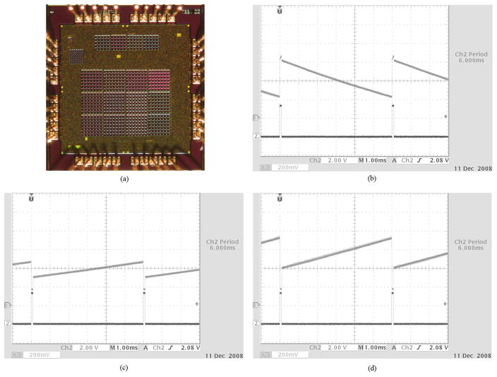
Fig. 3.
(a) Micrograph of the 1.5 mm × 1.5 mm die showing arrays of the test pixels and other test structures. Panels (b), (c), and (d) show measured pixel outputs from the 3T APS, 10 fF CTIA APS, and the 5 fF CTIA APS, respectively. All APS pixels are implemented with n-well/p-sub photodiodes. The CTIA APS was covered by an OD 1.8 neutral density filter attenuating incident light by a factor of 62.5.

