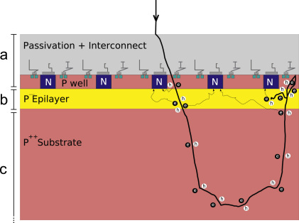
Fig. 14.
Schematic of MAPS CMOS detector. The pixel spacing is determined by the spacing between diodes formed by the well doped areas indicated in blue. The division into three layers used in the simulations is indicated and consists of: (a) passivation and heavily doped wells; (b) sensitive layer consisting of the lightly doped epilayer; and (c) heavily doped substrate. The track of an incident electrons is shown illustrating the problem with backscattering from the substrate in a non-backthinned detector. The diffusive collection by the reverse biased well diodes of mobile electrons generated in electron-hole pair excitations is indicated.

