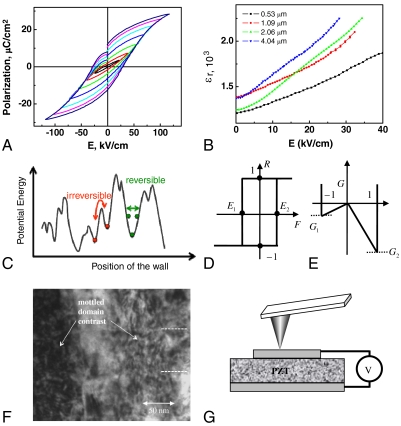
Fig. 1.
(A) A family of minor and major hysteresis loops measured using large area electrodes showing the evolution of hysteresis with the excitation window for the 1.09 μm PZT film used in this study. (B) Field dependence of the dielectric constant vs. ac field for different PZT film thicknesses. For these films, the permittivity dependence on dc bias, Vac, and frequency are all consistent with domain wall motion being the dominant contributor to the observed nonlinearity. (C) Landscape of potential energy of a domain wall. The circles denote the positions of domain walls. Applied electric fields can cause the walls to move either reversibly within a well or irreversibly between wells, (D) In a Preisach model, hysteresis behavior of material is determined by the distribution function ρ(E1,E2) of the elementary hysterons, where E1 and E2 are lower (higher) coercive fields. This hysteresis loop corresponds to double-well free energy shown in (E). The Rayleigh limit corresponds to ρ(E1,E2) = const. Despite extensive studies, the relationship between the pinning potential (C) and statistical descriptions (D, E) is elusive. (F) Section from a bright field TEM micrograph of the cross-section of a 1 μm thick film, showing the domain structure. The large scale defects parallel to the substrate result from the original spin and crystallization steps. (G) Schematics of experimental set-up illustrating sample geometry and PFM measurements.

