Figure 1.
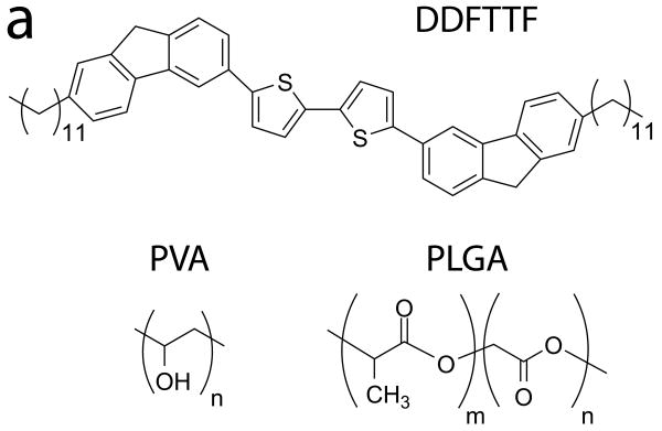
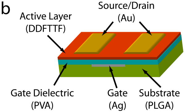
Materials Selection and Device Configuration of Organic Thin Film Transistors. (a) The chemical structures of the semiconductor (DDFTTF), the dielectric (PVA), and the substrate (PLGA) are shown. (b) These materials are processed into devices in top-contact configuration as shown. Briefly, PLGA was melt-processed into substrates approximately 1 × 1 cm2 in area and 2 mm in thickness. Silver gate contacts were evaporated through a shadow mask. PVA dielectrics were spin coated from solution followed by thermal evaporation of DDFTTF semiconducting layers and gold source-drain contacts. The final device geometry contained channel lengths of 50 μm and a W/L ratio of 20.


