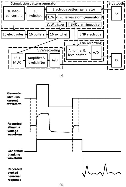
Fig. 1.
(a) Functional block diagram of the wearable controller. Abbreviations: A/D and D/A—analog-to-digital and digital-to-analog converters, MUX—multiplexer, Rx—reception of data, Tx—transmission of data, V-to-I—voltage-to-current. (b) Temporal sequence of the generated current stimulus waveform and blanking waveform relative to the recorded stimulus voltage waveform and evoked potential response.

