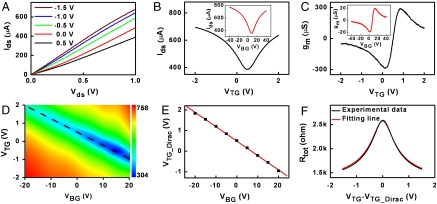
Fig. 4.
Room temperature electrical properties of the top-gated graphene device using Al2O3 nanoribbon as the gate dielectric. (A) Ids-Vds output characteristics, the channel width and length of the device is 2.1 μm and 4.1 μm. (B) Transfer characteristics at Vds = 1 V for the device using top and back gate (Inset). (C) Transconductance gm as a function of top-gate voltage VTG, the inset shows the gm vs. VBG. The plots indicate the top gate gm is about 15 times higher than the back-gate gm. (D) Two-dimensional plot of the device conductance at varying VBG and VTG bias. The unit in the color scale is μS. (E) The top-gate Dirac point VTG_Dirac at different VBG. (F) Experimental plot (Black Line) and modeling fitting (Red Line) of Rtot vs. VTG-VTG_Dirac relation to derive the contact resistance and carrier mobility.

