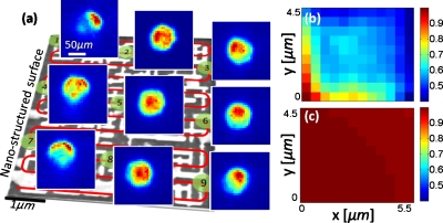
Figure 2.
(a) Calibration process of a nanostructured transmission surface is outlined. Several far-field calibration images of the patterned chip shown in Fig. 1b are also provided. (b) Cross-correlation coefficients of the first calibration frame against all the other calibration images of the same chip are illustrated. (c) Same as part (b), except this time it is measured for a bare glass substrate without the nanopattern. Significantly higher cross-correlation observed in (c) for closely spaced points is the reason for limited spatial resolution of conventional lensfree incoherent imaging without the nanopattern. Nanostructured surfaces break this correlation as shown in (b) to achieve a significantly better resolution.

