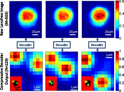
Figure 3.
Experimental proof-of-concept of lensfree on-chip imaging using the nano-structured surface of Fig. 1b is demonstrated. Top row shows the lensfree diffraction images of the objects sampled at the CCD for three different incoherent objects. Each diffraction image contains M=355 pixels. Bottom row shows the compressive decoding results of these raw diffraction images to resolve subpixel objects on the chip. For comparison, the inset images in the bottom row show regular reflection microscope images of the objects, which very well agree with the reconstruction results. Note that the red colored regions of the inset images refer to the gold coated area with no transmission, and therefore the reconstructions only focus to the dark regions of the chip (at the center of the inset images) that are nanopatterned.

