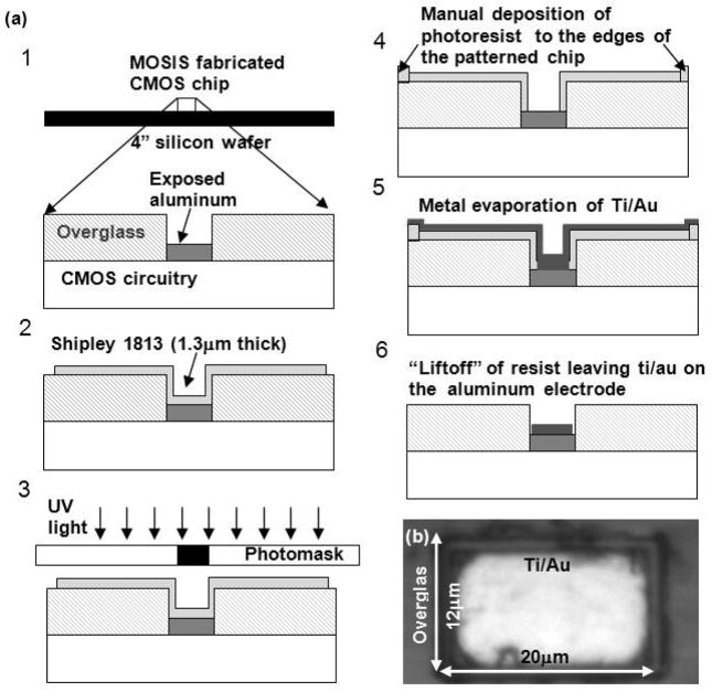
Fig. 2.
(a) Schematic of the process flow for deposition of polarizable material on Al electrodes using photolithography. There are six steps associated with the post-CMOS fabrication using photolithography. In the first step, the CMOS die is placed on a 4″ carrier wafer coated with photoresist and baked. The following steps illustrated in the figure do not show the carrier wafer. (b) Microscopic image of a single Al electrode coated with 10 nm Ti layer for adhesion and 200 nm Au layer.

