Fig. 3.
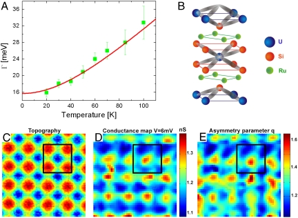
Kondo lattice. (A) Temperature dependence of the Kondo resonance width Γ extracted from the fits in Fig. 2B. The red line represents the temperature dependence for a single Kondo impurity described in the text, which results in a Kondo temperature TK = 129 ± 10 K. (B) Crystal structure of URu2Si2 indicating the different atomic layers and a schematic of the orbitals that bond the Si atoms to the U atoms. (C) A high-resolution constant current topography of 4 × 4 atoms taken at 18 K. (D) Conductance map at 6 mV (Kondo resonance energy) corresponding to the topography in C showing atomic scale modulations. (E) The dimensionless q(r) map on the same area as in C obtained by fitting the spectra at each location to a Fano line shape. The larger values of q (indicating higher tunneling probability to the Kondo resonance) lie in between the atomic sites as depicted by the black square.

