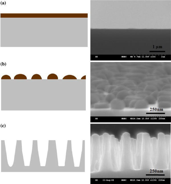
Figure 1.

Fabrication process flow for tapered subwavelength antireflection structures:aPt/Pd alloy thin film deposition with a thickness of 10 nm;bthermally dewetted Pt/Pd alloy nanodot etch mask formed at an elevated temperature; andcformation of tapered subwavelength antireflection structures after RIE
