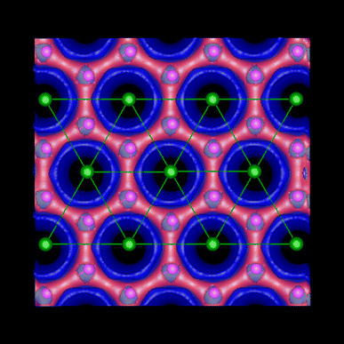
Figure 1.

The atomic structure of graphene/Si superlattice, with Si atoms on top, projected onto the graphene plane, overlaid with two contour plots of the total charge density. The contour of the 80% maximum (red) reveals the charge distribution on graphene, and the 20% contour (blue, drawn with 40% opacity) shows the charge distribution on the Si sheet
