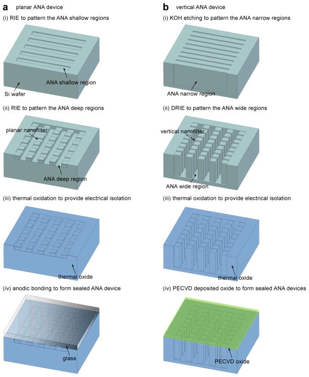
Figure 1.
Schematic of the fabrication process for both the planar and vertical ANA devices. In brief, for the planar ANA device (a), the shallow and deep regions of the ANA are defined and etched into a Si wafer using photolithography and RIE. KOH etching is performed to etch through the wafer for creating buffer access holes (not shown). A thick thermal oxide layer is grown to provide an electrical isolation between the conductive Si substrate and buffer solution. Finally, the ANA device is sealed by bonding a Pyrex wafer on the front surface of the silicon wafer. For the vertical ANA device (b), the narrow and wide regions of the ANA are defined and etched into a Si wafer using photolithography, DRIE, and wet anisotropic KOH etching. Then a thermal oxide layer is grown to further decrease the nanofilter gap size to a desired value. Finally, a uniform PECVD oxide layer is deposited to seal the ANA structure.

