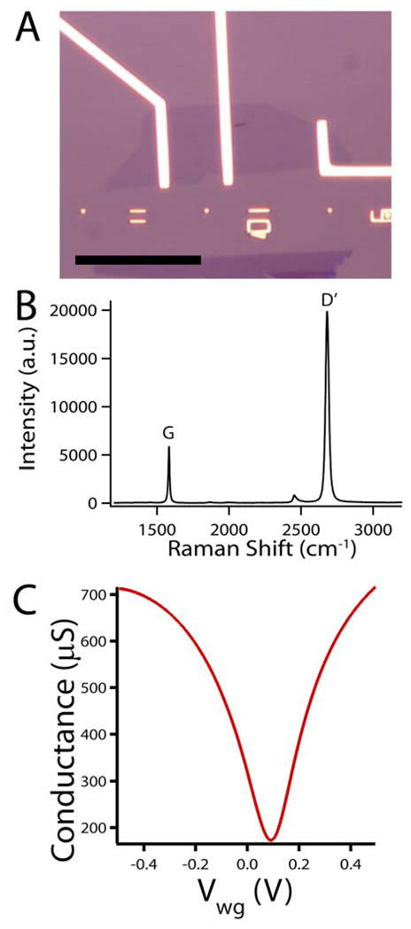
Figure 2. Graphene device fabrication and characterization.

(A) optical image of a single layer graphene FET, scale bar is 30μm. The interference contrast is consistent with a single graphene layer. (B) Corresponding Raman spectrum of the graphene device in panel A. (C) Water gate response of a typical Gra-FET.
