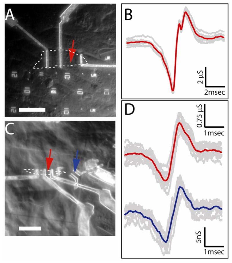
Figure 4. Size effect on recorded signals.

(A) Optical microscope image of PDMS/cells interfaced with large flake graphene FET. Graphene flake outline is marked by white dashed line, measured device is marked by red arrow. Scale bar is 30μm. (B) Recorded averaged peak (red) and raw data (grey traces) for the Gra-FET and cell in (A). Twelve raw peak signals (gray traces) were aligned in time and then averaged.28 (C) Optical microscope image of PDMS/cells interfaced with smaller flake graphene FET and SiNW FET. Graphene flake outline is marked by white dashed line, measured graphene device is marked by red arrow and measured SiNW device is marked by blue arrow. Scale bar is 13.6 μm. (D) Thirteen raw signal peaks (gray traces) from the Gra-FET (upper data) SiNW-FET (lower data) devices marked by red and blue arrows, respectively, in (C). The peaks were aligned in time28 and the average was plotted in red and blue, respectively.
