Fig. 1.

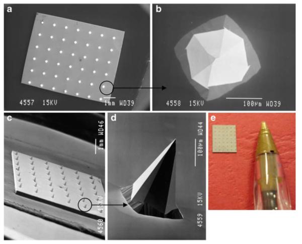
SEM images taken of a typical silicon MN array from directly above (a), of a single MN from above (b), of an array from the side (c) and of an individual MN from the side (d). Digital photograph of a typical silicon MN array (e).

SEM images taken of a typical silicon MN array from directly above (a), of a single MN from above (b), of an array from the side (c) and of an individual MN from the side (d). Digital photograph of a typical silicon MN array (e).