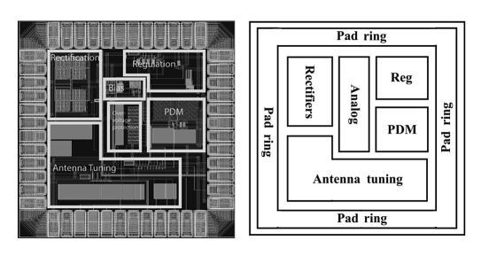
Figure 3.
Layout plot of the 1 × 1 mm2ASIC control chip (left), and the associated explanatory diagram (right). The sensor data was sampled and converted for transmission on a serial digital wireless link using a pulse density modulation. The low sampling rate (one per five minutes) combined with the low power allowance inspired the use of time domain encoding in which the intervals between digital signals were used to encode analog data without the need for a full analog to digital conversion.

