Abstract
While nanostructures of organic conductors have generated great interest in recent years, their nanoscale size and shape control remains a significant challenge. Here we report a general method for producing a variety of oligoaniline nanostructures with well-defined morphologies and dimensionalities. 1-D nanowires, 2-D nanoribbons, and 3-D rectangular nanoplates and nanoflowers of tetraaniline are produced by a solvent exchange process in which the dopant acid can be used to tune the oligomer morphology. The process appears to be a general route for producing nanostructures for a variety of other aniline oligomers such as the phenyl-capped tetramer. X-ray diffraction of the tetraniline nanostructures reveals that they possess different packing arrangements, which results in different nanoscale morphologies with different electrical properties for the structures. The conductivity of a single tetraaniline nanostructure is up to two orders of magnitude higher than the highest previously reported value and rivals that of pressed pellets of conventional polyaniline doped with acid. Furthermore, these oligomer nanostructures can be easily processed by a number of methods in order to create thin films composed of aligned nanostructures over a macroscopic area.
INTRODUCTION
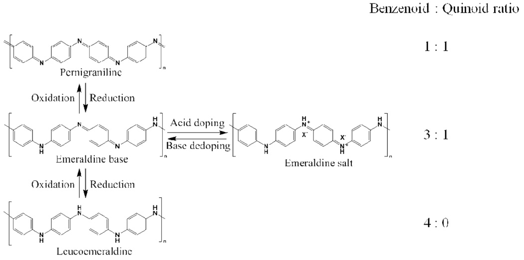
One-dimensional (1-D) nanostructures of molecular organic conductors and conducting polymers have attracted growing attention in recent years due to their solution processability, easily tunable electronic properties, and potential use in many novel applications.1,2,3 In addition, these materials can shed light on the structure-property relationships for this unique class of nanomaterials.1 Among the family of conducting polymers, polyaniline has been extensively studied due to its unique oxidation-reduction chemistry, environmental stability, biocompatibility, and for its simple acid-base doping-dedoping process as illustrated in Figure 1.4–8 Nanofibers of polyaniline have demonstrated enhanced performance in applications such as chemical sensors, catalysis, and supercapacitors due to their high surface area and porous nature.9–11 However, the performance and stability of many devices are governed by how molecules or polymer chains assemble in the solid state.12,13 The lack of order at the chain level has limited polyaniline nanofibers from being integrated into electronic devices that require high carrier mobility and stability such as organic field-effect transistors and solar cells. These applications are currently dominated by molecular semiconductors that can often self-assemble into highly ordered nanowires or nanoribbons.1,2,14 Moreover, polyaniline nanofibers typically possess low aspect ratios and are highly flexible, which makes the fabrication of single-wire devices and post-synthetic alignment difficult.
Figure 1.
The oxidation-reduction chemistry of polyaniline: The fully reduced form of polyaniline, known as leucoemeraldine, can be half-oxidized to form emeraldine or fully oxidized to form pernigraniline. The electrically insulating emeraldine base form of polyaniline (conductivity ≤ 1×10⁻¹⁰ S/cm) can be doped with a strong acid to produce the electrically conducting emeraldine salt form of polyaniline (conductivity ≥ 1 S/cm). This process can be reversed by adding a strong base. Note that only the emeraldine oxidation state of polyaniline can be doped to form an electrically conducting polymer. Tetraaniline is obtained when n = 1 and therefore is the smallest oligomer unit that can fully represent the structure of polyaniline.
In contrast to polyaniline, oligomers of aniline are capable of forming ordered extended structures; crystals of low molecular weight oligomers have already been characterized.15–18 However, compared to polyaniline, reports on oligoanilines are sparse, especially in regards to generating nanoscale structures and/or improving their electrical conductivity.19–21 Oligoanilines have generally been reported to possess low conductivities ranging from 10−6 to 10−2 S/cm for tetraaniline in pressed pellet form.20,21 However, the bulk conductivity of a conducting polymer is governed by both the transport properties within a molecular chain and between chains.16,19,22,23 In this regard, oligoanilines have great potential for improvements in the material’s interchain transport properties. Reports on the conductivity of oligoanilines from a pressed pellet are therefore typically low due to the fact that interchain transport is not optimized. Oligoanilines also represent an interesting middle ground between polyaniline and molecular semiconductors because oligoanilines retain the chemical properties of the polymer, e.g., the acid-base doping-dedoping chemistry (see Figure 1), while also possessing properties typically associated with molecular semiconductors especially in regard to monodispersity and self-assembly.
The most important oxidation state of polyaniline is the emeraldine base form, since it can be doped by strong acids to create the conducting form, which can be readily and reversibly reduced to the insulating emeraldine base form as shown in Figure 1. The emeraldine oxidation state of polyaniline possesses three benzene rings for every quinoid ring. Amine/phenyl-capped tetraaniline, hereafter referred to as tetraaniline (see Table S1 for nomenclature and structures of aniline oligomers), therefore represents an important model compound for polyaniline because structure-wise, it is the shortest oligomer that can represent the emeraldine oxidation state. Here we report a general and versatile method for producing structurally ordered and well-defined oligoaniline nanostructures via the self-assembly of tetraaniline and other aniline oligomers in their most conductive emeraldine salt oxidation state. Exquisite nanoscale morphology and dimensionality control is demonstrated via a simple dopant-induced process. The conductivities of these nanostructures are measured via single wire, ribbon, or plate measurements. The values observed are two orders of magnitude higher than previously reported pressed-pellet values for oligoanilines and are comparable to that of conventional polyaniline.20,21
EXPERIMENTAL SECTION
Synthesis
N-phenyl-1,4-phenylenediamine and N, N’-diphenyl-1,4-phenylenediamine were purchased from Sigma-Aldrich and TCI Chemicals, respectively, and were used without further purification. Tetraaniline was synthesized via a previously reported route.24 In brief, iron (III) chloride dissolved in 0.1 M HCl was mixed with stoichiometric amounts of N-phenyl-1,4-phenylenediamine (aniline dimer) suspended in the same solvent. After 2 hours of vigorous stirring, the suspension was filtered and repeatedly washed with 0.1 M HCl until the filtrate became clear. The solid was collected and dedoped with 0.1 M ammonium hydroxide. The dedoped crude product was reduced to the leucoemeraldine oxidation state with hydrazine and recrystallized from ethanol three times in order to purify the product. Tetraaniline was then re-oxidized to the emeraldine base form with one equivalent of ammonium peroxydisulfate (APS). The final product was characterized by UV-Vis, Fourier transform infrared (FT-IR) spectroscopy, and matrix-assisted laser desorption/ionization-time of flight (MALDI-TOF) mass spectroscopy (Figure S1). Phenyl-capped octaaniline was synthesized by a condensation reaction in an inert atmosphere via a previously reported route.25 Phenyl-capped tetraaniline was synthesized using the same method with tetraaniline replaced by N-phenyl-1,4-phenylenediamine as the starting material. Characterizations for these two oligomers are shown in Figure S2 and S3, respectively.
Process for producing nanostructures
In a typical process, 2.0 mg of finely powdered tetraaniline is added to a solvent mixture comprised of 1.0 mL of ethanol and 4.0 mL of an aqueous acidic solution. The mixture is shaken for a few seconds and then left undisturbed for 4 to 5 days. Less ethanol is used for N-phenyl-1,4-phenylenediamine and N,N’-diphenyl-1,4-phenylenediamine than tetraaniline since they have a higher solubility in ethanol. Duration of the processes varied slightly depending on the oligomer. Molecular structures and common abbreviations for the aniline oligomers are summarized in Table S1 along with the detailed conditions for their nanostructure formation. Each reaction mixture was purified by dialysis against deionized water for approximately one day. A small amount of granular debris often precipitated out and was visible at the bottom of the vial. The debris can be readily removed by agitating the vial since the granular debris settles out from the dispersion quickly, while the nanostructures remain well-dispersed for a lengthy period of time. As a result, the top nanostructured dispersion can be collected into a different container and the debris that accumulates at the vial bottom discarded.
Microscopy
Scanning electron microscopy (SEM) and transmission electron microscopy (TEM) samples were prepared by drop-casting one to two drops of a diluted oligoaniline dispersion onto a piece of silicon wafer or a TEM grid, respectively. SEM images were taken with a JEOL JSM-6700 Field Emission scanning electron microscope, and TEM images were taken with a FEI/PHILIPS CM 120 transmission electron microscope.
Other characterization techniques
Powder X-ray diffraction patterns of the tetraaniline nanostructures were taken on a Panalytical X'Pert Pro X-ray powder diffractometer with a scan rate of 2 degrees/min. Sodium chloride was used as an internal standard for the crystallite size calculations using the Scherrer equation. MALDI samples were prepared with 2,5-dihydroxybenzoic acid (DHB) as the matrix and the spectra were taken on an Applied Biosystems Voyager-DE-STR MALDI-TOF spectrometer. FT-IR samples were prepared with FT-IR grade KBr and the spectra were taken with a JASCO FT/IR-420 spectrometer. UV-vis-NIR (near infrared) spectra of the nanowire dispersion were taken with a quartz cuvette that has a 1 mm light path-length on a Shimadzu UV-3101 PC UV-vis-NIR Scanning Spectrophotometer.
Single wire measurements
Bottom-contact devices were fabricated for all single wire, ribbon, and plate measurements. Gold electrodes were thermally deposited on a Si/SiO2 substrate with a 300 nm SiO2 layer to create channels that are 2–10 µm in length. One drop of oligoaniline dispersion was drop-cast onto the electrodes, and the nanowires, nanoribbons, or rectangular nanoplates were allowed to settle for a few seconds. The rest of the droplet was then quickly removed with flowing nitrogen and the devices blown thoroughly dry. Measurements were carried out directly after deposition using a standard probe station under ambient conditions.
RESULTS AND DISCUSSION
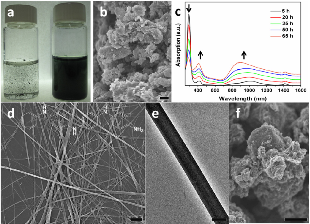
Tetraaniline synthesized by previously reported methods possesses a granular, agglomerated morphology (Fig. 2b). However, nanostructures of tetraaniline can be grown by adding this granular powder to a mixture of 0.1 M HCl and ethanol, which is then left undisturbed for 4 to 5 days. During this time, large particles are observed that initially precipitate to the bottom of the vial and gradually turn into the green, doped form of tetraaniline. This material slowly disperses into the surrounding medium. At the end of this process, only doped tetraaniline is observed floating in the solvent. The mixture forms a stable dispersion upon simple agitation (Fig. 2a). SEM and TEM images of the resulting dispersion show that long, non-woven nanowires with high aspect ratios are created during this process (Fig. 2d, 2e). The nanowires typically range in diameter from 70 to 200 nm and are up to hundreds of microns long. A UV-vis-NIR spectrum of the resulting tetraaniline nanowires in the emeraldine salt form dispersed in water is shown as the “65 h” curve in Figure 2c, and a full spectrum that extends into the near infrared (NIR) up to 3000 nm is shown in Figure S4. The as-synthesized dedoped tetraaniline in its emeraldine base form dissolved in ethanol is presented in Figure S1c and is consistent with previous work on tetraaniline.7,24
Figure 2.
(a) Photographs show a mixture of tetraaniline, ethanol, and 0.1 M HCl at the beginning of the process (left vial) and the green tetraaniline nanowire dispersion produced at the end of 4 days (right vial). Both vials were agitated prior to taking the photos; (b) A scanning electron microscope (SEM) image of the as-synthesized tetraaniline powder; (c) UV-Vis spectra obtained at the given time intervals during the course of nanowire assembly; (d) An SEM image of a network of tetraaniline nanowires. The molecular structure of tetraaniline is shown across the top of the image; (e) A transmission electron microscope (TEM) image of a single tetraaniline nanowire; and (f) the results of the same process carried out in a mixture of ethanol and water in the absence of doping acids. Scale bars: 1 µm.
Literature reports indicate that π-conjugated molecules can form well-defined morphologies and molecular arrangements through non-covalent interactions such as π-π stacking and hydrogen bonding. Controlled aggregation of molecules through these non-covalent interactions in a non-solvent or in a mixture of a non-solvent and a good solvent can lead to the formation of nanowires or nanoribbons.1,14 Tetraaniline nanowires may form in an analogous process to that known for other molecular semiconductor nanowires such as perylene tetracarboxylic diimide derivatives.14,26,27 Although tetraaniline is not soluble in an acidic aqueous solvent, it can be doped in this environment. Tetraaniline is, however, soluble in common organic solvents such as ethanol. The solubility and the degree of aggregation of tetraaniline in different liquids can be easily tuned by adjusting the ratio of the two solvents/non-solvents. Upon increasing the aqueous component, the enhanced solvent polarity can create solvophobic association between the aromatic rings, which promotes extended π-π stacking, in a similar manner to how surfactants and amphiphilic molecules assemble.26,28 Tuning the solvent ratio thus allows for controlled aggregation and stacking of tetraaniline molecules. With a solvent mixture of 4:1 (v/v) of an aqueous solution of HCl (a non-solvent) and ethanol (a good solvent), tetraaniline molecules assemble into an extended superstructure consisting of nanowires. During this process, bulk tetraaniline powder slowly disperses into the solvent to form a suspension of tetraaniline nanowires. Control experiments carried out in a solely acidic aqueous environment leads to poorly-defined structures (see Fig. S5), which illustrates the importance of achieving the correct solvent polarity from a mixture of solvents.
The nanowire growth process requires approximately four days in order for directional molecular self-assembly to occur which has been suggested as a factor in forming ordered nanostructures for other molecules such as perylene diimide and pentacene.14,26,27,29 Non-covalent forces such as hydrogen bonding can modulate the directional nature of nanowire formation.27,30 Although high aspect ratio nanowires are obtained in a solvent mixture of ethanol and 0.1 M HCl, an identical process carried out in a mixture of ethanol and water without any dopant acid only yields agglomerates (Fig. 2f). Tetraaniline remains in its initial emeraldine base oxidation state in water, but becomes the protonated emeraldine salt form when the process is performed in an acid solution. This may be a result of extra hydrogen bonding associated with the protonation which has been proposed as a driving force to regulate supramolecular organization.31,32 The transition in oxidation state from the initial emeraldine base form of tetraaniline to the final emeraldine salt form was monitored in situ via UV-vis-NIR spectroscopy during the course of nanowire assembly. UV-vis-NIR spectra were collected 5 hours into the process and then every 15 hours until the relative peak ratios stopped changing (Fig. 2c). At 5 hours, agglomerates that resemble the morphology of the as-synthesized tetraaniline are observed, and nanowires become the dominant product after 65 hours. Three peaks are present. The peak at 290 nm corresponds to the π → π* transition. This transition typically appears between 350–360 nm for doped polyaniline;33,34 however, it undergoes a blue shift to 290 nm due to the much shorter conjugation length of tetraaniline compared to polyaniline. Absorptions at 420 nm and around 950 nm are ascribed to the polaron → π* and π → polaron band transitions, respectively, indicating that the nanowires are in their conductive emeraldine salt form.33 The weak peak around 1420 nm is due to water absorption.35 As the assembly process progresses, the spectra changes significantly with a defined isosbestic point at 325 nm. The drastic decrease in the ratio of the 290 nm peak to the 420 nm peak indicates that the π → π* transition energy is greatly reduced as the tetraaniline molecules equilibrate into a more preferred aggregate phase with extended π-π stacking as nanowires form. A similar effect has been observed in nanostructures of molecular conductors.30 On the other hand, the ratio of the 420 nm peak to the 290 nm peak increases throughout the process, indicating an increase in doping level as more polarons are injected into the π* band as assembly progresses. Simultaneously, the broad peak at ∼900 nm which extends over several hundreds of nm from the visible to the NIR region also increases in intensity compared to the 290 nm peak. The broadening of this asymmetric peak is associated with the increasing linearity of polyaniline which leads to increased polaron delocalization.33,34,36 The increase in absorption of this broad peak during tetraaniline nanowire assembly suggests that the intermolecular stacking between aniline tetramers leads to delocalization of carriers because of the enhanced π-π orbital overlapping. Therefore, the overall change in the ratios of peak absorptions indicates that tetraaniline molecules rearrange themselves from the initially agglomerated morphology into an extended, more thermodynamically favorable array with better carrier transport during the process of nanowire assembly.
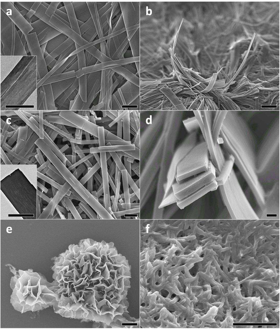
Size and shape control of 1-D organic nanostructures remains a significant challenge within the field of organic conductors and continues to draw increasing interest. For example, studies have shown that using different doping acids during the synthesis of polyaniline nanofibers can change their diameter. When synthesized in 1.0 M HCl, polyaniline nanofibers typically have diameters around 30 nm, while in 1.0 M camphorsulfonic acid (CSA) the diameters average 50 nm.37 For oligomers, their organization into extended supramolecular structures can be controlled by using different dopants that have different sizes. As shown in Figure 2, 1-D nanowires are formed when HCl is used as the doping acid; however, as the dopant is changed to HNO3, 2-D nanoribbons are obtained (Fig. 3a and 3b). Using HClO4 induces the formation of well-defined 3-D rectangular-shaped nanoplates (Fig. 3c and 3d), while H2SO4 produces tetraaniline molecules that pack into nanoflowers consisting of well-organized clusters of 2-D nanosheets (Fig. 3e).
Figure 3.
(a) An SEM image of tetraaniline nanoribbons obtained when 1.0 M HNO3 is used as the doping acid. The inset shows a TEM image of a single ribbon; (b) An edge-on view of the nanoribbons; (c) An SEM image of rectangular-shaped tetraaniline nanoplates produced using 0.5 M HClO4 as the doping acid. The inset shows a TEM image of a nanoplatelet; (d) An SEM cross-sectional view of the nanoplates; (e) An SEM image of nanoflowers produced using 1.0 M H2SO4 as the doping acid; and (f) an SEM image of inter-connected nanofibers obtained when 1.0 M CSA is used as the doping acid. Scale bar: 100 nm for (d), 1 µm for all the others.
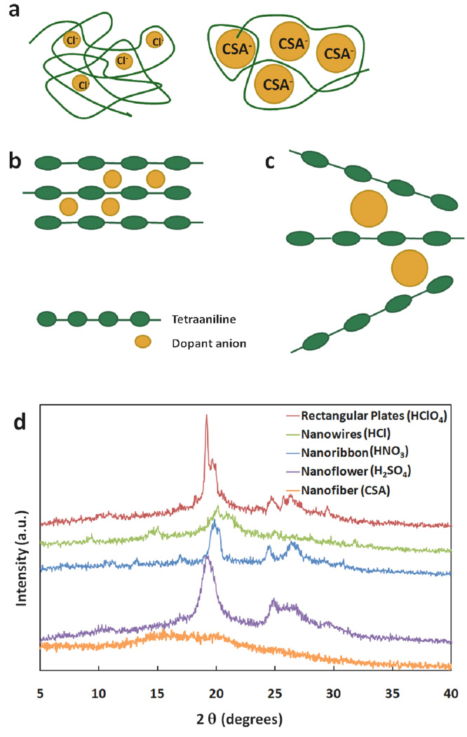
The exquisite dopant-induced nanoscale control of the size and shape of aniline-based oligomers and polymers can be explained by examining and comparing the structural differences between the polymer and the oligomer. When polyaniline or oligoaniline is doped with an acid, the imine nitrogens become protonated and the negatively charged dopant anions reside near the positively charged nitrogens due to ionic attractions (Fig. 1). The size of the dopant anions thus influences the interchain packing distance and ultimately the supramolecular morphology. Polyaniline molecular chains are long and semi-rigid in sections; thus, dopant anion size does not have a large effect on the supramolecular structure observed for polyaniline since individual dopants only have a local effect on the polymer chains (Fig. 4a).38 Thus, changing the dopant acid during the synthesis of polyaniline nanofibers primarily changes diameter, but has little affect on superstructure. However, oligoanilines such as tetraaniline are discreet, compact molecules. Consequently, the size of the dopant anion has a much more profound effect on the packing distances between tetraaniline molecules (Fig. 4b). This effect can be observed in the X-ray diffraction (XRD) patterns for the different tetraaniline nanostructures (Fig. 4d). For each of the four structures, the most intense peak in the X-ray diffraction pattern is centered around 2θ = 20°, which has been ascribed to the periodicity parallel to the polymer chain.39–42 When HCl is used as the doping acid to induce nanowire formation, Cl− ions remain between the chains, which results in a peak at 2θ = 20.00° corresponding to a d-spacing of 4.22 Å. This peak shifts to 2θ = 19.87° for HNO3 doped nanoribbons, which indicates an increase in d-spacing to 4.46 Å. This is consistent with the fact that NO3− is a larger dopant anion than Cl−. Nanoflowers doped by H2SO4 and rectangular nanoplates doped by HClO4 have even larger d-spacings of 4.62 Å and 4.63 Å, respectively, as HSO4− and ClO4− ions are larger than NO3−and Cl−.43 To further illustrate the impact of dopant anion size, when a very large doping acid such as camphorsulfonic acid (CSA) is employed, only poorly-defined, agglomerated tetraaniline nanofibers are obtained (Fig. 3f). This is due to the fact that CSA anions are bulky in size and they prevent oligomers from packing into ordered and discrete supramolecular structures (Fig. 4c). Their lack of packing order is evident in the corresponding XRD pattern, which does not have well-defined peaks and thus suggests an amorphous structure (Fig. 4d). Note that aside from the amorphous CSA-doped agglomerated nanofibers, the intensity of the X-ray diffraction patterns indicate that the nanowires are the least crystalline form of nanostructure, while the rectangular nanoplates and nanoribbons are far more crystalline. Such observations are consistent with the physical appearances of the nanostructures. Nanoflowers also produce intense diffraction peaks despite the fact that they do not appear as ordered as the nanoplates or nanoribbons. This can be attributed to the crystallinity of the stacked 2-D sheets/“petals” that comprise the nanoflowers. The Scherrer equation has been applied to assess the crystallite sizes of the four different morphologies. Using sodium chloride as an internal standard, the crystallite sizes were calculated to be 17 Å for the nanowires, 44 Å for the nanoribbons, 91 Å for the rectangular nanoplates, and 25 Å for the nanoflowers. Since the calculated crystallite sizes for the nanowires and the nanoflowers are well below the 50 Å accuracy limit of the Scherrer equation, the data for these materials should be considered qualitative. The rectangular nanoplates have the longest crystallite coherence length, approximately one-tenth of their average physical thickness, further confirming their high crystallinity. The calculated crystallite size of the nanoribbons falls between the nanocrystalline nanowires/nanoflowers and the more crystalline nanoplates, in agreement with the XRD data. In addition, well-defined 2θ peaks around 26o that correspond to classical π-π stacking between aromatic rings are observed for the more crystalline nanoribbons, nanoplates, and nanoflowers, further demonstrating that π-π stacking is likely an important driving-force for nanostructure assembly. This is also supported by the previously discussed in situ UV-vis-NIR analysis (Figure 2c), where a greatly reduced π → π* transition energy is observed due to the formation of extended π-π stacking as nanostructures assemble.
Figure 4.
(a) An illustration of the polymer chain conformation typically found which is compactly coiled when a small doping acid such as HCl is used (left); the chain becomes more expanded when doped with a bulky doping acid such as CSA and processed in certain solvents (right).38 (b) The dopant anions likely reside between the tetraaniline molecular chains; therefore, the packing distance will be affected by the size of the anions. (c) Tetraaniline molecular chains do not pack well when a bulky doping acid such as CSA is used as the tetramers are prevented from arranging themselves into extended structures; and (d) X-ray diffraction patterns of nanowires (top), nanoribbons (second), rectangular nanoplates (third), nanoflowers (fourth), and agglomerated nanofibers (bottom).
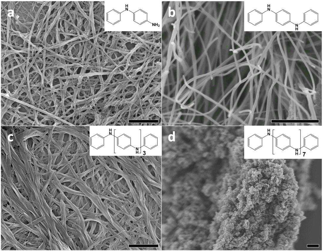
The synthetic methodology presented here appears to be a general and versatile route for producing nanostructures of other aniline oligomers. For example, nanowires of aniline dimer (N-phenyl-1,4-phenylenediamine) and phenyl-capped aniline dimer (N,N’-diphenyl-1,4-phenylenediamine) are obtained by the same method when HCl is used as the doping acid, and phenyl-capped tetraaniline forms a mixture of nanowires and narrow nanoribbons under the same conditions (Fig. 5a to 5c). Unfortunately, when the same approach is applied to phenyl-capped octaaniline, only agglomerates are obtained (Fig. 5d), likely due to the fact that the increase in chain length results in a molecule with more polymer-like characteristics so that its size and shape cannot be as readily controlled by this process.
Figure 5.
SEM images of (a) aniline dimer nanowires; (b) phenyl-capped aniline dimer nanowires; (c) phenyl-capped aniline tetramer nanowires and nanoribbons; and (d) phenyl-capped octaaniline agglomerates produced under the same experimental conditions that form tetraaniline nanostructures. Scale bar: 1 µm. Insets show the molecular structures of the corresponding aniline oligomer.
Electrical transport studies on HCl-doped nanowires, HNO3-doped nanoribbons, and HClO4-doped rectangular nanoplates were performed in order to determine the conductivities of each of these nanostructures. Previous studies on the conductivity of doped tetraaniline measured on pressed pellets have proven to be disappointing: the conductivity ranges from 10−6 to 10−2 S/cm depending on the synthetic method and doping acid used.20,21 Our studies confirm that bulk tetraaniline has a conductivity of only 3 × 10⁻³ S/cm. However, pressed-pellet measurements represent the lower boundary for conductivity for oligoanilines due to high contact resistance between the numerous junctions between the nanostructures that can cause the conductivity to appear lower than the intrinsic conductivity of a single wire or ribbon. Measuring the conductivity of a single nanowire, nanoribbon or nanoplate therefore represents a method to determine the intrinsic conductivity of oligoaniline nanostructures.
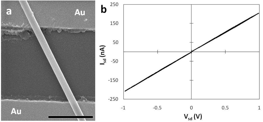
Figure 6a shows a representative SEM image of an Au bottom-contact device constructed from a single tetraaniline nanowire. The nanowire was drop-cast across the source and drain electrodes from a freshly prepared dispersion of tetraaniline nanowires in water. The nanowires were allowed to deposit for a few seconds, and the rest of the droplet was quickly blown away by nitrogen flow, followed by taking an immediate measurement. This method of deposition reduces the amount of solvent impurities that would be left behind from solvent drying, which would decrease the quality of the measurements. Tetraaniline nanoribbon and nanoplate devices were fabricated in the same fashion. Figure 6b shows a typical I-V curve for a single nanowire device through a two-probe measurement. All measurements were carried out under ambient conditions with a standard semiconductor probe station. The linearity of the curve indicates that the tetraaniline nanostructures exhibit ohmic behavior. The conductivity of each nanostructure was calculated using the slope of the I-V plot along with the length of the nanostructure that bridges the source and drain electrodes. The actual length and width (or diameter in the case of a nanowire) of each channel were measured by SEM, and the thickness of the ribbon or plate was acquired through tilted SEM measurements assisted by AFM analysis when needed. The conductivity of a single nanowire was found to be as high as 0.3 S/cm, and that for a nanoplate and nanoribbon were as high as 0.5 S/cm and 1.1 S/cm, respectively. This trend is consistent with the X-ray diffraction patterns and the crystallite coherence length obtained using the Scherrer equation as the nanowires were the least crystalline morphology with the smallest crystallite size, while the nanoribbons and rectangular nanoplates were much more crystalline and have larger crystallite sizes. The fact that the nanoplates have lower conductivity than the nanoribbons, despite their higher crystallinity and longer crystallite coherence length, can be ascribed to their poor contact with the Au electrodes since the plates are not as long or flexible as the ribbons. For measurements on different devices, conductivities in the range of 0.1 – 1.1 S/cm were obtained for nanoribbons. Such distribution of values was also observed for the nanowires and nanoplates. This range of variation can be partly attributed to (1) the differences in contact quality at the Au electrode-nanoribbon interfaces that are often associated with bottom contact devices, and (2) solvent impurities and/or microscopic debris trapped at the aforementioned interfaces. On this basis, it is evident that the conductivities we report here could likely be further improved if the contact quality and other issues are addressed; for instance, fabricating four-probe top-contact devices to reduce contact resistance. Despite these issues, the conductivity of the nanoribbon exhibits a two order of magnitude increase from the highest value reported previously for tetraaniline,21 and a three order of magnitude increase from the method we followed for synthesizing bulk aniline tetramer.24 It is worth emphasizing that the conductivity of the nanoribbons rivals that of conventional polyaniline, which has a conductivity on the order of 100–101 S/cm.6,21,44 Such results clearly demonstrate that oligoanilines can be as highly conducting as the polymer once the interchain transport and the inter-domain transport components of bulk conductivity are optimized. The improved interchain transport as a result of the increased intermolecular order is evident from the in situ UV-vis-NIR analysis and the XRD patterns. The conductivity may be further enhanced if a balance between the oligomer chain length and interchain packing is achieved.
Figure 6.
(a) An SEM image of a representative bottom-contact device fabricated from a single tetraaniline nanowire on a Si substrate covered by a 300 nm thick SiO2 dielectric layer. The channel lengths between the Au electrode pairs were varied from 2 µm to 10 µm; a 2 µm channel length is shown. Scale bar = 1 µm.
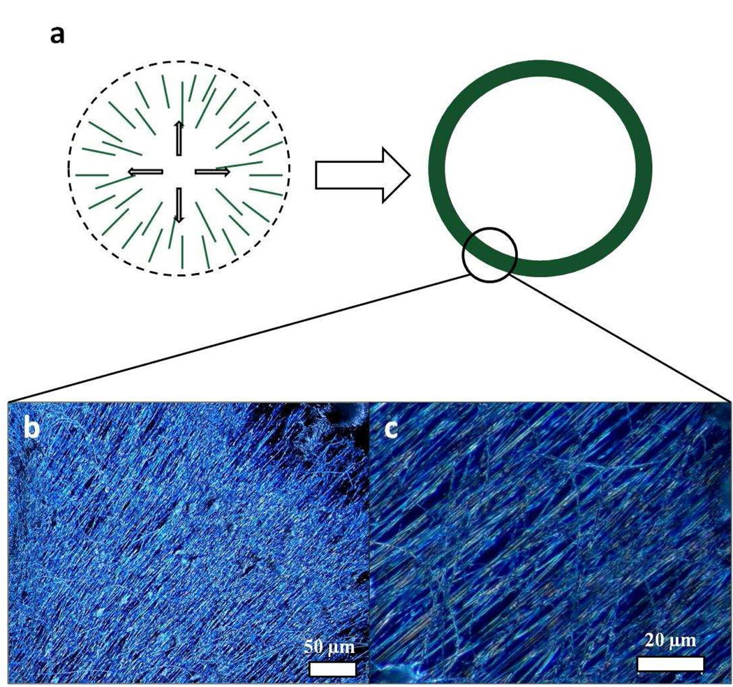
The inter-domain transport in a nanowire film could be further improved by assembling the randomly oriented oligoaniline nanostructures into oriented functional arrays onto a variety of substrates. This has been difficult to achieve for polyaniline nanofibers which typically form an interpenetrating network of nanofibers which makes individual fibers or wires difficult to separate. Fortunately, the oligoaniline nanowires tend to be much more rigid with high aspect ratios leading to discreet fibers. Initial experiments indicate that they can be readily aligned using dewetting alignment, in which nanowires that possess high aspect-ratios can be deposited and aligned between the solvent front and the substrate as shown in Figure 7a.45–47 Through this evaporation-induced assembly process, the tetraaniline nanowires are drawn towards the direction of the droplet evaporation, causing the nanowires to align in a radial fashion. The solution in the center continuously replenishes the solvent as it evaporates at the edges, thus increasing the nanowire deposition density at the edge of the droplet. A ring with high deposition density is formed as the droplet dries. Optical microscope images of a section of the ring are shown in Figure 7b and c, illustrating the high degree of alignment and high deposition density. These aligned sections could be transferred to a desired substrate for further device fabrication. In addition to dewetting alignment, the microfluidic flow method48 is also applicable for the assembly of tetraaniline nanowires (Figure S6). Solution-based large-area alignment should facilitate directional carrier transport and greatly lower contact resistance versus their non-oriented counterparts,49–51 which could prove to be beneficial for high efficiency organic thin-film microelectronic devices or for transparent, flexible organic electrodes.
Figure 7.
(a) A schematic representation of evaporation-induced (dewetting) deposition and alignment between the solvent front and the substrate. (b) An optical micrograph taken in dark field shows a small section of the ring. The nanowires align in the drying direction. (c) A dark field optical micrograph showing a closer view of (b).
CONCLUSIONS
Nanostructured aniline oligomers have been produced through a novel, simple one-step method in which bulk oligoanilines self-assemble in a suitable binary solvent system. Supramolecular structures including nanowires, nanoribbons, rectangular nanoplates, and nanoflowers are obtained through a process in which the dopant induces a specific morphology in the oligoanilines. The variation in structures could prove useful for next-generation organic electronics; for example, the high surface area nanoflowers could be used for organic super-capacitors, while nanowires or nanoribbons could be well-suited for single-wire/ribbon nanoelectronic devices. Two-probe electrical measurements on single wires, ribbons, and plates reveal that the conductivity of the tetraaniline nanostructures increase by two orders of magnitude from the highest previously reported values for tetraaniline and now rival that of conventional polyaniline. This increase in conductivity from bulk tetraaniline is due to the increased intermolecular order as evidenced by XRD and in situ UV-vis-NIR analyses. The nanostructures can be readily assembled into thin films with orientation over a macroscopic area via a number of methods such as dewetting or microfluidic flow.
Supplementary Material
ACKNOWLEDGMENTS
We thank Sergey Prikhodko and Yujing Li for help with TEM, Sabah Bux and Michael T. Yeung for assistance with XRD, and Shan Jiang for help with graphics. Support for this research has been provided by the UCLA based Focused Center Research Program Functional Engineered NanoArchetectonics center (R.B.K.), an NIH Director’s New Innovator Award Program, part of the NIH Roadmap for Medical Research, through Grant 1DP2OD004342-01 (X.D.), and a National Science Foundation Integrative Graduate Education and Research Training: Clean Energy for Green Industry Fellowship DGE–0903720 (Y.W.).
Footnotes
Supporting Information Available: Characterization, part of the mechanistic study, and nanowire assembly through microfluidic flow. This material is available free of charge via the Internet at http://pubs.acs.org.
REFERENCES
- 1.Briseno AL, Mannsfeld SCB, Jenekhe SA, Bao Z, Xia Y. Mater. Today. 2008;11(4):38–47. [Google Scholar]
- 2.Mas-Torrent M, Rovira C. Chem. Soc. Rev. 2008;37:827–838. doi: 10.1039/b614393h. [DOI] [PubMed] [Google Scholar]
- 3.Roncali J, Leriche P, Cravino A. Adv. Mater. 2007;19:2045–2060. [Google Scholar]
- 4.Tran HD, Li D, Kaner RB. Adv. Mater. 2009;21:1487–1499. [Google Scholar]
- 5.Jang J. Emissive Mater.: Nanomater.: Adv. in Poly. Sci. 2006;199:189–259. [Google Scholar]
- 6.Huang J, Kaner RB. In: Handbook of Conducting Polymers. 3rd ed. Reynolds J, Skotheim T, editors. New York: Marcel Dekker, Inc; 2006. pp. 194–241. Chapter 7. [Google Scholar]
- 7.Li D, Huang J, Kaner RB. Acc. Chem. Res. 2009;42(1):135–145. doi: 10.1021/ar800080n. [DOI] [PubMed] [Google Scholar]
- 8.Zhang D, Wang Y. Mater. Sci. Eng. B. 2006;134:9–19. [Google Scholar]
- 9.Huang J, Virji S, Weiller B, Kaner RB. Chem: A Euro. J. 2004;10:1314–1319. doi: 10.1002/chem.200305211. [DOI] [PubMed] [Google Scholar]
- 10.Gallon BJ, Kojima RW, Kaner RB, Diaconescu PL. Angew. Chem. Int. Ed. 2007;46:7251–7254. doi: 10.1002/anie.200701389. [DOI] [PubMed] [Google Scholar]
- 11.Gupta V, Miura N. Mater. Lett. 2006;60:1466–1469. [Google Scholar]
- 12.DeLongchamp DM, Sambasivan S, Fischer DA, Lin EK, Chang P, Murphy AR, Fréchet JMJ, Subramanian V. Adv. Mater. 2005;17:2340–2344. [Google Scholar]
- 13.DeLongchamp DM, Kline RJ, Lin EK, Fischer DA, Richter LJ, Lucas LA, Heeney M, McCulloch I, Northrup JE. Adv. Mater. 2007;19:833–837. [Google Scholar]
- 14.Zang L, Che Y, Moore JS. Acc. Chem. Res. 2008;41(12):1596–1608. doi: 10.1021/ar800030w. [DOI] [PubMed] [Google Scholar]
- 15.Poncet M, Corraze B, Quillard S, Wang W, MacDiarmid AG. Thin Solid Films. 2004;458:32–36. [Google Scholar]
- 16.Zhou Y, Geng J, Li G, Zhou E, Chen L, Zhang W. J. Poly. Sci. Part B: Poly. Phys. 2006;44:764–769. [Google Scholar]
- 17.Baughman RH, Wolf JF, Eckhardt H, Shacklette LW. Synth. Met. 1988;25:121–137. [Google Scholar]
- 18.Shacklette LW, Wolf JF, Gould S, Baughman RH. J. Chem. Phys. 1988;88(6):3955–3961. [Google Scholar]
- 19.MacDiarmid AG, Zhou Y, Feng J. Synth. Met. 1999;100:131–140. [Google Scholar]
- 20.Wei Z, Faul CFJ. Macromol. Rapid Commun. 2008;29:280–292. [Google Scholar]
- 21.Surwade SP, Agnihotra SR, Dua V, Manohar N, Jain S, Ammu S, Manohar SK. J. Am. Chem. Soc. 2009;131:12528–12529. doi: 10.1021/ja905014e. [DOI] [PubMed] [Google Scholar]
- 22.MacDiarmid AG. Synth. Met. 1997;84:27–34. [Google Scholar]
- 23.Avlyanov JK, Min Y, MacDiarmid AG, Epstein AJ. Synth. Met. 1995;72:65–71. [Google Scholar]
- 24.Zhang WJ, Feng J, MacDiarmid AG, Epstein AJ. Synth. Met. 1997;84:119–120. [Google Scholar]
- 25.Lu FL, Wudl F, Nowak M, Heeger AJ. J. Am. Chem. Soc. 1986;108(26):8311–8313. [Google Scholar]
- 26.Che Y, Datar A, Balakrishnan K, Zang L. J. Am. Chem. Soc. 2007;129:7234–7235. doi: 10.1021/ja071903w. [DOI] [PubMed] [Google Scholar]
- 27.Balakrishnan K, Datar A, Naddo T, Huang J, Oitker R, Yen M, Zhao J, Zang L. J. Am. Chem. Soc. 2006;128:7390–7398. doi: 10.1021/ja061810z. [DOI] [PubMed] [Google Scholar]
- 28.Paramonov SE, Jun H-W, Hartgerink JD. J. Am. Chem. Soc. 2006;128:7291–7298. doi: 10.1021/ja060573x. [DOI] [PubMed] [Google Scholar]
- 29.Briseno AL, Mannsfeld SCB, Lu X, Xiong Y, Jenekhe SA, Bao Z, Xia Y. Nano Lett. 2007;7:668–675. doi: 10.1021/nl0627036. [DOI] [PubMed] [Google Scholar]
- 30.Würthner F. Chem. Commun. 2004:1564–1579. doi: 10.1039/b401630k. [DOI] [PubMed] [Google Scholar]
- 31.Stejskal J, Sapurina I, Trchova M, Konyushenko EN, Holler P. Polymer. 2006;47:8253–8262. [Google Scholar]
- 32.Wang Y, Tran HD, Kaner RB. J. Phys. Chem. C. 2009;113:10347–10349. [Google Scholar]
- 33.Xia Y, Wiesinger JM, MacDiarmid AG, Epstein AJ. Chem. Mater. 1995;7(3):443–445. [Google Scholar]
- 34.Rannou P, Gawlicka A, Berner D, Pron A, Nechtschein M. Macromolecules. 1998;31(9):3007–3015. [Google Scholar]
- 35.Irvine WM, Pollack JB. ICARUS. 1968;8:324–360. [Google Scholar]
- 36.MacDiarmid AG, Epstein AJ. Synth. Met. 1994;65:103–116. [Google Scholar]
- 37.Huang J, Kaner RB. J. Am. Chem. Soc. 2004;126:851–855. doi: 10.1021/ja0371754. [DOI] [PubMed] [Google Scholar]
- 38.MacDiarmid AG, Epstein AJ. Synth. Met. 1995;69:85–92. [Google Scholar]
- 39.Tang Q, Wu J, Sun X, Li Q, Lin J. Langmuir. 2009;25:5253–5257. doi: 10.1021/la8038544. [DOI] [PubMed] [Google Scholar]
- 40.Anilkumar P, Jayakannan M. J. Phys. Chem. B. 2009;113:11614–11624. doi: 10.1021/jp9043418. [DOI] [PubMed] [Google Scholar]
- 41.Wang J, Wang J, Dai Z, Wang Z, Zhang F. Synth. Met. 2009;159:1583–1588. [Google Scholar]
- 42.Winokur MJ, Mattes BR. Macromolecules. 1998;31:8183–8191. [Google Scholar]
- 43.Conway BE. Ionic Hydration in Chemistry and Biophysics. Amsterdam: Elsevier; 1981. pp. 59–74. [Google Scholar]
- 44.Peng C-Y, Kalkan AK, Fonash SJ, Gu B, Sen A. Nano Lett. 2005;5(3):439–444. doi: 10.1021/nl048083v. [DOI] [PubMed] [Google Scholar]
- 45.Huang J, Fan R, Connor S, Yang P. Angew. Chem. Int. Ed. 2007;46:2414–2417. doi: 10.1002/anie.200604789. [DOI] [PubMed] [Google Scholar]
- 46.Deegan RD, Bakajin O, Dupont TF, Huber G, Nagel SR, Witten TA. Nature. 1997;389:827–829. doi: 10.1103/physreve.62.756. [DOI] [PubMed] [Google Scholar]
- 47.Hameren Rv, Schön P, Buul AMv, Hoogboom J, Lazarenko SV, Gerritsen JW, Engelkamp H, Christianen PCM, Heus HA, Maan JC, Rasing T, Speller S, Rowan AE, Elemans JAAW, Nolte RJM. Science. 2006;314:1433–1436. doi: 10.1126/science.1133004. [DOI] [PubMed] [Google Scholar]
- 48.Huang Y, Duan X, Wei Q, Lieber CM. Science. 2001;291:630–633. doi: 10.1126/science.291.5504.630. [DOI] [PubMed] [Google Scholar]
- 49.Long Y, Chen Z, Wang N, Ma Y, Zhang Z, Zhang L, Wan M. Appl. Phys. Lett. 2003;83(9):1863–1865. [Google Scholar]
- 50.Long Y, Zhang L, Ma Y, Chen Z, Wang N, Zhang Z, Wan M. Macromol. Rapid Commun. 2003;24:938–942. [Google Scholar]
- 51.Li G, Martinez C, Janata J, Smith JA, Josowicz M, Semancik S. Electrochem. Solid-State Lett. 2004;7(10):H44–H47. [Google Scholar]
Associated Data
This section collects any data citations, data availability statements, or supplementary materials included in this article.


