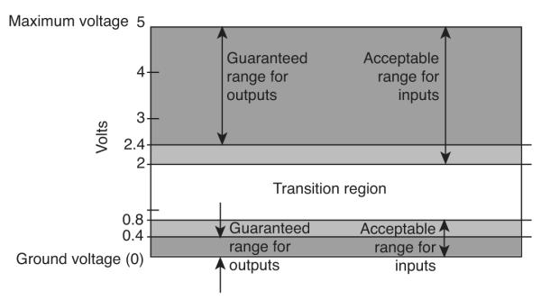
Figure 1.
Voltage bands corresponding to 1 (voltages greater than 2), and 0 (voltages less than 0.8). These ranges define the limits for acceptable inputs to a logic gate. Output voltage criteria are stricter. Greater reliability is achieved when logic component manufacturers adhere to this scheme, because one gate in a chain can effectively clean up extreme noise in its inputs before propagating its output.

