
Figure 1.
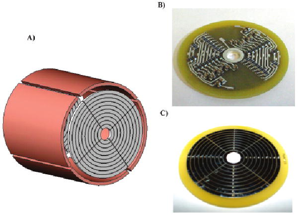
(A) A conceptual representation of the eTREC design. (B) A photograph of the backside of the eTREC trap plate including installed resistor and capacitor components. (C) A photograph of the front side of the eTREC trap plate revealing the conductor pattern for the rings and quadrants.