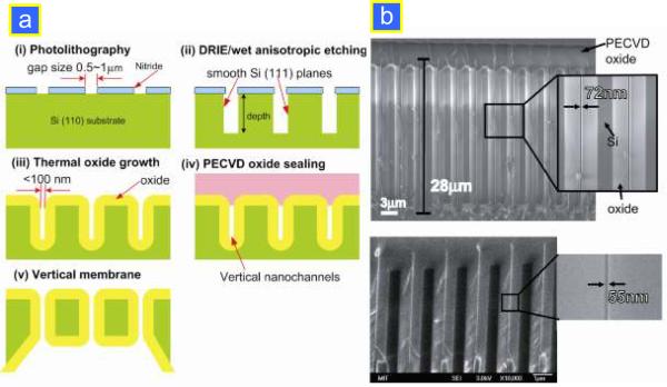
Figure 6.
(a) Schematic diagram of fabricating vertical nanochannels:14 (i) photolithography defines pattern structures; (ii) vertical trenches with smooth sidewalls are etched by either DRIE or anisotropic wet etching (KOH); (iii) thermal oxide growth further decreases the gap size; (iv) uniform PECVD oxide is deposited to seal narrow trenches; (v) backside etching of the Si wafer yields thin membranes over a wide area (~6 inch wafers). (b) Cross-sectional SEM micrographs of slot-like vertical nanochannels with a uniform gap size of 72 nm and 55 nm. The channels are etched by KOH etching and have a depth of 28 μm. The channels are completely sealed by depositing 3 μm thick PECVD oxide.

